multilayer pcb prototype

Price: $39.60

Product Description

High-performance Multilayer PCB Prototypes with up to 18 layers. Made by top-notch manufacturing techniques, these boards have precise tolerances, signal integrity and reliable performance. Samples ready in as quickly as 3 days. Designed to support custom stack-ups and controlled impedance. They are a perfect fit for aerospace, medical, telecom and advanced electronics applications.

Shipping

Shipping costs and delivery timelines to be negotiated—please contact us for a detailed quote.

Payments and Security

Your payment is handled through a secure system; we do not retain or have access to your credit card information.

Easy Return & Refund

If your order is missing or delivered with defect, you may request a refund. Our support team will respond within 24 hours.

Layer CountsUp to 18 layers
Base MaterialFR4
Bord Thickness 1.6 mm
Maximum PCB Size570*850mm
PCB Size Tolerance±0.2-0.3mm
Min.Hole Size0.1mm
Min.Line Width4mil
Copper Weight21oz
Surface FinishENIG, HASL, OSP are optional
CertificateUL , IPC-6012, RoHS, ISO 9001, ISO14001
Add a review
multilayer pcb prototype multilayer pcb prototype
Rating*
0/5
* Rating is required
Your review
* Review is required
Name
* Name is required
Add photos or video to your review
* Please tick the checkbox to proceed
* Please confirm that you are not a robot
0.0
Based on 0 reviews
5 star
0%
4 star
0%
3 star
0%
2 star
0%
1 star
0%
0 of 0 reviews

Sorry, no reviews match your current selections

Frequently Asked Questions

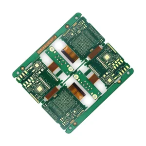
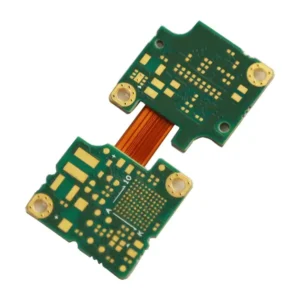
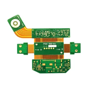
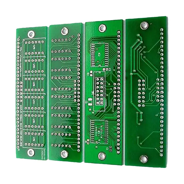
A multilayer PCB prototype is a test version of a printed circuit board with layers more than two conductive layers. It helps check out the design, layout and performance before mass production.
We accept Gerber, ODB++, Eagle and Altium and other industry standard formats. If you aren’t sure, our engineers can convert or review your files.
By optimizing the stackup design, using low-loss materials, and ensuring precise impedance matching (±5%), our engineers can ensure signal integrity in high-speed multilayer PCBs.
Yes! We support laser-drilled blind vias, staggered/buried vias, and any-layer HDI for ultra-compact, high-performance designs.
Sure. We provide free DFM/DFA review for our customers, your design is optimized for manufacturing.
Yes! All our prototypes use RoHS-compliant materials and lead-free ENIG/HASL finishes.