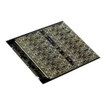
Product Description
Sequential lamination with stepped via technology enables our 16 layer HDI Step PCBs to achieve maximum routing density. Designed for advanced, high-speed electronic systems, they ensure excellent signal performance, reduced crosstalk, and smooth layer transitions. Ideal for applications such as 5G, AI, medical imaging, telecom, and advanced computing. Fully certified to ISO 9001 and IPC Class 3 standards, ensuring reliability in mission-critical systems.
Shipping
Shipping costs and delivery timelines to be negotiated—please contact us for a detailed quote.
Payments and Security
Your payment is handled through a secure system; we do not retain or have access to your credit card information.
Easy Return & Refund
If your order is missing or delivered with defect, you may request a refund. Our support team will respond within 24 hours.
| Layer Counts | 16 layers |
| Base Material | High-Tg FR4, Rogers, Polyimide |
| Bord Thickness | 0.8-2.0mm |
| Maximum PCB Size | 570*670mm |
| Minimum PCB Size | 10*10mm |
| PCB Size Tolerance | ±0.2-0.3mm |
| Min.Hole Size | 0.1mm |
| Min.Line Width | 4mil |
| Copper Weight | 4oz |
| Surface Finish | ENIG, HASL, OSP are available |
| Certificate | UL , IPC-6012, RoHS, ISO 9001, ISO14001 |
 16 layer hdi step pcb
| 5 star | 0% | |
| 4 star | 0% | |
| 3 star | 0% | |
| 2 star | 0% | |
| 1 star | 0% |
Sorry, no reviews match your current selections
Contact Us