When you need to choose a circuit board, you have many options. From basic rigid boards to sophisticated flexible boards, from straightforward single-layer boards to intricate multi-layer boards. Are you aware of how to choose the best one? No matter which type of PCB you choose, they are made up of different numbers of PCB layers, and each PCB layer has its specific function. You will find a comprehensive guide to circuit board layers in this blog. Let’s explore each PCB layer role together.
What Are PCB Layers?
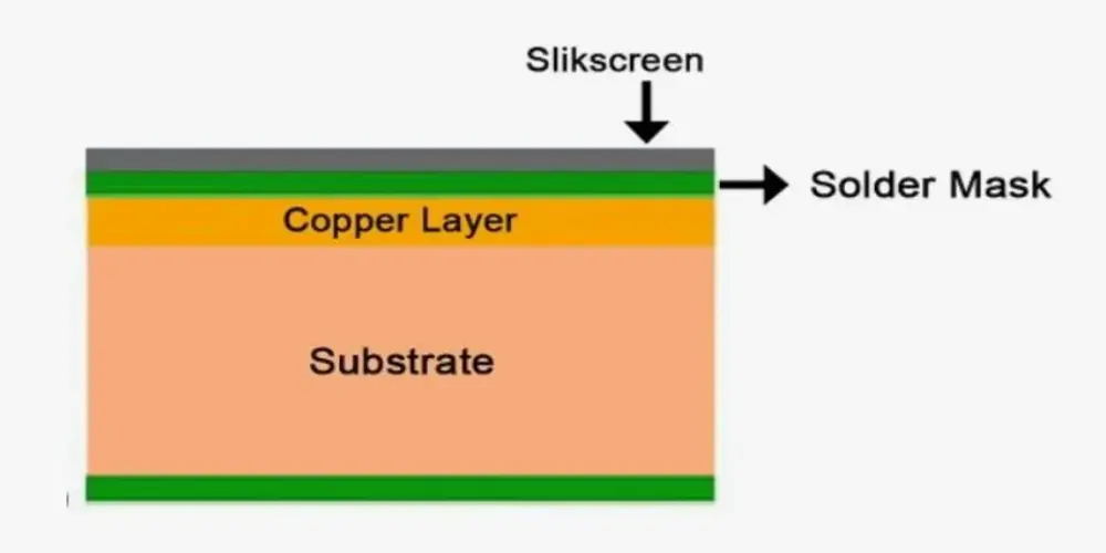
PCB layers refer to the conductive layers and insulating layers that make up the PCB. These layers typically include a conductive copper layer, insulated substrate layer, protective solder mask layer, and labeling silkscreen layer, among others. Multilayer PCBs allow for much more complex circuitry simply by sandwiching these circuit board layers together. Increasing the number of layers allows the PCB to provide more complex electrical connections and higher functions. It can fit more components in a smaller size, hence improving the density and whole performance of the circuit board.
Types of PCB Layers
In this section, we will explain each PCB layer in detail. You can get a thorough grasp of their function.
Substrate Layer
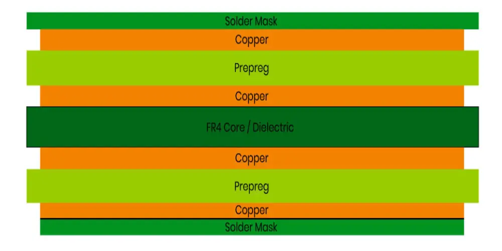
The core substrate primarily serves two roles: electrical insulation and mechanical support. It is usually composed of a non-conductive material, a base on which the conductive layers and other components can be built. Materials commonly used for substrates are: FR-4, polyimide, a glass-reinforced epoxy laminate, medal core, ceramic core, etc. FR-4 is widely used in various circuit boards due to its superior mechanical properties, electrical properties, thermal stability, etc. Polyimide is often used in circuit boards that require bending and high-temperature resistance due to its flexibility and excellent thermal stability.
Copper Layer
The conductive layer is usually a thin copper layer laminated on the substrate to provide a channel for the flow of electrical signals. It is etched to remove the unwanted parts, and finally form the desired circuit pattern. We usually refer to the number of copper layers when discussing the number of layers in a PCB. Single-sided PCBs only have a conductive copper layer while double-sided PCBs have two copper layers. The copper layer thickness depends on power and performance needs. Thicker copper layers provide better current carrying capacity, lower resistance, and improved heat dissipation, but also increase the difficulty of fine pitch trace design and manufacturing.
Solder Mask Layer
The solder mask, which is often green, is a protective polymer PCB layer that covers the copper surface. This coating’s primary purpose is to shield the copper traces from oxidation and corrosion. In order to avoid short circuits between traces, it also offers electrical insulation. During the PCB assembling process, this coating helps accurately locate solder joints and reduces the risk of solder bridges, ensuring that components can be installed correctly. This PCB layer can improve the environmental adaptability of the circuit board, and resist the erosion of moisture and pollutants, thereby extending the service life of the PCB.
Silkscreen Layer
The silkscreen layer is the text identification PCB layer on the circuit board. It is usually printed on the surface of the circuit board in white, which contrasts with the green solder mask layer. The main function of this PCB layer is to help engineers and technicians quickly identify the location, function, and pin definition of each component on the board by marking various words, numbers, and symbols, facilitating the assembly, testing, and later maintenance of the circuit board.
Prepreg
Prepreg is a semi-cured dielectric material made of fiberglass cloth impregnated with epoxy resin. In the PCB manufacturing process, prepreg is mainly used to bond the layers (such as copper foil and core substrate) together and provide the necessary electrical insulation between them. After the heat and pressure treatment, the prepreg will be fully cured.
Different Types of PCBs Based on Layer Count
Single-Layer PCBs
This design only has traces on one side, and the other side is used to install electronic components. When wiring, it is necessary to avoid wire crossing. If necessary, this can be solved by jumpers or 0-ohm resistors. Its simple structural characteristics make it particularly suitable for large-scale and simple electronic products.
Here are the outstanding advantages:
- Easier design and production
- Cheap alternative
- Applicable to low complexity products
Double-Layer PCBs
Single-layer PCBs still have some limitations, and you can choose double-layer PCBs at this time. Double-layer PCBs are covered with conductive copper layers on both sides of the substrate. This structure allows electronic components to be mounted on both sides, which can achieve higher circuit density and more complex designs. Double-layer PCB has a good balance of cost and performance and is suitable for more complex, more flexible, and smaller product requirements.
Here are the outstanding advantages:
- High circuit density
- Small board size and low weight
- Improved signal integrity and EMI shielding
Complex Multilayer PCBs
Mmulti-layer PCBs have more than 2 copper layers. The copper layers are separated by insulating materials and pressed together through a hot pressing process. The design of the multilayer structure will be able to provide more complicated PCB layouts within the small space. Though the process of making this advanced PCB is more complex, it has turned into an indispensable part of today’s high-end electronic products.
Four-Layer PCBs
A 4-layer PCB contains 4 conductive layers. The inner two copper layers are often used as power and ground layers, and the top and bottom layers are used for mounting components and signal routing. The multi-layer construction introduces a way of connecting electrically between layers with vias that improve signal integrity and heat dissipation. In fact, for special design requirements, the stack-up of four-layer PCBs could flexibly change.
Six-Layer PCBs
A 6-layer PCB would add two additional signal layers as compared to a 4-layer PCB. In the PCB stack-up, there are four routing layers with two internal layers assigned to one for the ground plane and the other for the power plane. This structure would heavily manage EMI simply by well-allocating high- and low-speed signals between different layers of the PCB. This can optimize routing efficiency and reduce the signal crosstalk for complex circuit designs.
Here are the outstanding advantages:
- Better EMI shielding and minimize crosstalk problems
- Higher circuit density and more compact design
- Improved thermal management
- Decreased power supply noise
Why Are Multilayer PCBs Designed with Even Layers?
You might have a better idea of multilayer PCBs after reading the introduction above. Do you note that the PCBs we introduce are all even-numbered-layer PCBs?Here will give 3 reasons why most PCB manufacturers choose to design and produce multilayer PCBs with an even PCB layer.
Cost-Effective Design
Odd-layer PCBs are fewer in terms of the number of copper and insulating layers, but the total cost of their manufacture is far more expensive than even-layer PCBs. Odd-layer PCBs require non-traditional lamination core bonding techniques. The outside layer requires extra treatment that may result in scratches and etching errors, while the inner layer receives the same treatment. To most manufacturers, odd layers are a special manufacturing process. Because of the specific production process of this PCB, it requires professional engineers in its treatment process, leading to higher labor costs, low productivity, and an increased number of trial-and-error costs.
Balanced Structure for Warping Resistance
For cooling after lamination of multi-layer circuit boards, the PCB will warp due to different layer tensions. In odd-numbered PCBs, there exist two composite PCBs with dissimilar structures that increase the potential for bending. The risk can be avoided through a balanced stack-up of a PCB. In certain cases, it is within an acceptable specification in terms of a degree of warping, though it will certainly cause inefficiency during subsequent processing, thereby increasing total cost.
We can also understand that 4-layer PCBs are easier to control warping than 3-layer PCBs, and the warping can be controlled below 0.7% (IPC 600 standard). In actual processes, designers will also tend to design odd-numbered PCBs as even-numbered PCBs.
Even Layers for Better Interference Resistance
Multilayer boards are made of alternately stacked copper foil and substrate. The distance between each layer of copper foil and the substrate can be kept relatively uniform and stable. It can minimize signal transmission delay and interference. The odd-numbered layer design will increase the distance between some layers, affecting the signal transmission. That is why an even-numbered layer design is commonly used.
How to Determine the Number of PCB Layers?
When figuring up the PCB layer number, keep in mind these four key factors.
- Budget Consideration: First of all, consider your project budget. PCBs with one or two sides are less expensive to manufacture. PCBs with many layers, however, will cost a little more.
- Performance Requirement: Is your PCB used for a sophisticated or simple product? If it is just a simple function, then a single-layer or double-layer PCB can be used without any problem. In case of a higher performance requirement, multilayer PCBs become an ideal alternative. The PCB layer number can be decided ultimately depending on the complication of the project.
- Space Limited: Estimate the space available for the PCB. If it is small, you want a higher layer count PCB that can fit components and routing requirements.
- Acceptable Lead Time: If you order a large number of PCBs, will the delivery time meet your expectations? Compared with multi-layer PCBs, single-layer and double-layer PCBs have simpler structures that need much shorter times in manufacturing. Multilayer PCBs require longer production times due to their complex structures.
Takeaways
With a deep understanding of the specific purpose of each PCB layer, you can easily master complex PCB structures. This can help you choose the perfect PCB according to your project needs and achieve the best balance between product performance and cost. Please get in touch with UnityPCB’s expert team if you have any questions concerning the PCB layer.
UnityPCB has nearly 20 years of PCB manufacturing experience, and we can provide you with multilayer PCBs of up to 18 layers. We are committed to providing high-quality PCB manufacturing services, and each PCB will be rigorously tested to ensure first-class quality.