PCB etching is an indispensable step in the PCB manufacturing process. Its purpose is to create conductive pathways on the PCB to form electrical connections between components. Yet, how is etching performed on circuit boards? Do you actually know what it is? In this blog, we will cover the fundamentals of PCB etching, including the entire process, and inform you about different etching techniques.
What Is PCB etching?
Etching PCB board refers to a process to remove unwanted copper from printed circuit board. Once all the extra copper on your PCB is removed, you’ll have only the circuit you need. It’s a critical fabrication step where a simple copper-clad board will become a working circuit board by defining precise electrical paths. This process enables proper component connections, prevents short circuits, and allows for compact circuit designs that are essential in modern electronics manufacturing.
The Two Main PCB Etching Techniques
There are two primary types of PCB etching methods: wet etching and dry etching. Each method has its features, and we should consider specific requirements such as precision, material properties, and production scale to decide which one to use.
Wet Etching
In the wet etching method, the PCB is dipped in a chemical solution that dissolves away unwanted copper from the copper clad laminate, leaving behind the circuit pattern you want. The solution itself can be either acid or alkaline:
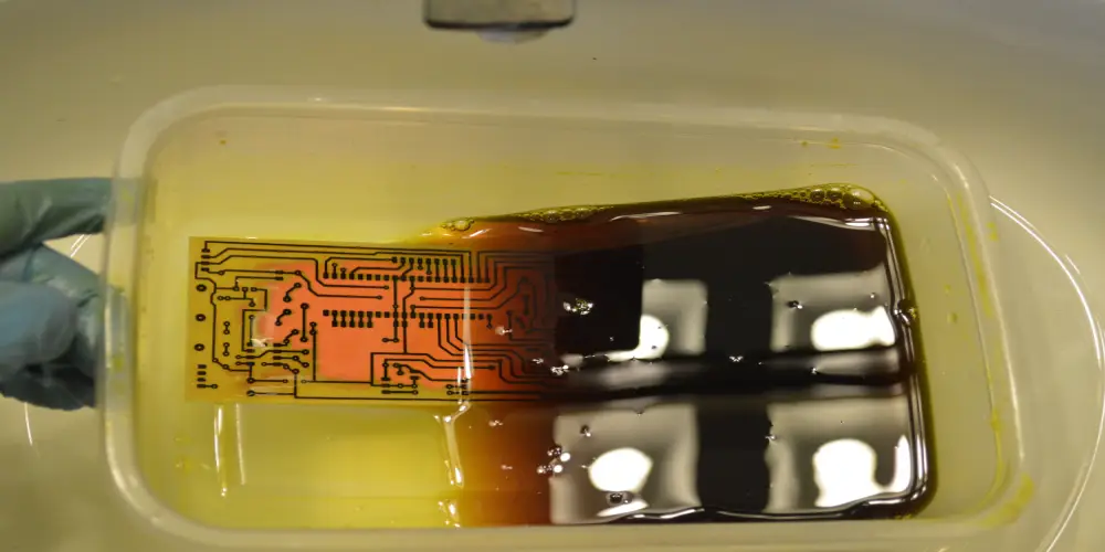
- Acidic Etching
During the acidic etching process, the PCB is exposed to a ferric chloride or hydrochloric acid to dissolve the copper. When standard PCBs are concerned, this method is very efficient and has a relatively low cost, which makes it a popular choice for low to medium volumes production. However, it results in a rougher surface finish and is quite hazardous when handling these chemicals, as they are highly corrosive.
- Alkaline Etching
Whereas alkaline etching uses a solution containing alkali-based chemicals such as ammonium persulfate. This method is gentler on the copper and generally producing more even etching results over acidic etching. Also, it is more environmentally friendly as producing less hazardous waste and better suited to high precision applications e.g. high frequency PCBs, or sensitive electronics.
Dry Etching
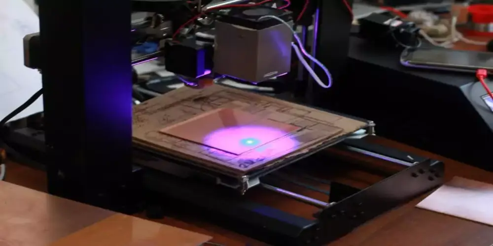
The more advanced process is dry etching, which etches the PCB using either plasma or lasers. Unlike wet etching, which uses liquid chemicals, its removal of unwanted copper is achieved by using gases or lasers
- Plasma Etching
Plasma etching is when a gas (such as oxygen or chlorine) is ionized into plasma inside of a vacuum chamber. The copper is broken down by the reactive ions in the plasma being removed. Plasma etching is used on microelectronics or multilayer PCB devices often for fine, intricate circuit pattern. In addition, it is also cleaner since it produces less waste as compared to wet etching methods.
- Laser Etching
In laser etching, a high-power laser beam is used to vaporize or burn the unwanted copper on the PCB. With its high precision features, the method is suitable for PCBs with highly complex designs such as HDI boards. Though it is expensive compared to other techniques, it is not commonly used for large-scale production.
Wet Etching vs. Dry Etching: A Quick Comparison
| Feature | Wet Etching | Dry Etching |
| Process | Uses chemical solutions (acid/alkaline) to etch the PCB. | Uses gases, plasma, or lasers to etch the PCB. |
| Precision | Less precise, suitable for simpler designs. | Highly precise, ideal for fine lines and complex designs. |
| Cost | Cost-effective for large-volume production. | More expensive due to the need for specialized equipment. |
| Environmental Impact | Generates chemical waste, requires disposal. | Produces less chemical waste, more eco-friendly. |
| Applications | Common in mass production of standard PCBs. | Used for high-precision and advanced PCBs, such as in medical or aerospace applications. |
| Complexity | Relatively simple process with minimal technical skill needed. | Requires specialized knowledge and advanced machinery. |
PCB Etching Process: 7 Steps Involved
- Prepare the PCB: Before PCB etching, surface should be cleaned. The board should be cleaned out any dirt, oil or contaminants. And then put masking material on your PCB where you want to keep the copper.
- Select an etching technique: Choosing the etching technique according to specific requirement. If the etching uses the chemical, then cover the entire surface of the PCB with a brush or spray bottle.
- Monitor the etching process: You need to watch the entire etching process carefully. Etching time depends on type of etchant used and thickness of PCB and solution temperature.
- Rinse the PCB: Afterwards, we should rinse the PCB with water in order to get rid of any remaining etchant on the PCB.
- Remove the masking material: After the PCB dries, you can take off the masking material to see your completed circuit.
- Clean the PCB: If the PCB has any residue left, then clean with an alcohol or degreaser.
- Inspect the PCB: Finally, check the PCB carefully for correct circuit pattern, and ensure no defects are present on the PCB.
Conclusion
Etching PCBs is still one of the most important steps in fabricating good quality boards. It is the foundation for all successful PCBs to guarantee that your circuit paths will run as precisely intended. Knowing different etching methods can help you decide which is best for your requirements, price and schedule.
If you’re a beginner on a PCB project and you need some help on the etching process, our team at UnityPCB is here to help you! We have experience in both traditional and advanced etching methods. Contact us now to find out how we can support your projects.