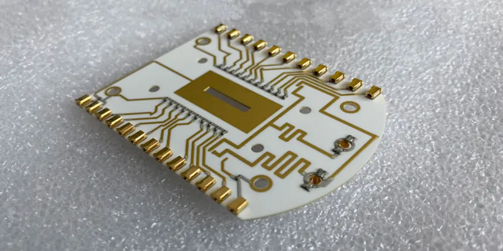
With the development of the electronics industry, ceramic PCB, as a new type of solution, provides more possibilities for electronic product design. Ceramic PCB can meet the needs of miniaturization of modern electronic products and provide better performance. In this blog, we will introduce the materials, types, manufacturing processes, advantages, and more of ceramic circuit boards in depth.
What Is Ceramic PCB?
Ceramic PCB uses ceramic materials like aluminum oxide, aluminum nitride, or beryllium oxide to replace the traditional FR4 substrate materials through a direct sintering process. Its thermal conductivity is also significantly higher than that of metal core PCB. Ceramic circuit board which offers excellent electrical insulation, low dielectric constant, and high-frequency performance, is an ideal solution for high-power, and high-frequency applications.
Various Types of Ceramic PCB Substrate Materials
When you choose the ceramic base materials to produce PCB, you need to pay more attention to PCB thermal conductivity and CTE. Let’s explore three main types of ceramic PCB substrate materials together.
Substrate Materials | Thermal Conductivity ((W/m·K)) | CTE ((ppm/°C)) |
| Aluminum Nitride | 150-180 W/mK | 4.5-5.5×10–⁶/°C |
| Alumina | 18-36 W/mK | 6-8×10–⁶/°C |
| Beryllium Oxide | 184-300 W/mK | 6.5-7.5×10–⁶/°C |
Aluminum Nitride (AIN)
Aluminum nitride is a high-performance ceramic material. It is especially suitable for applications with high power, high frequency, and high-reliability requirements, like high-power LEDs, automotive sensors, and integrated circuits.
Alumina/Aluminum Oxide (Al₂O₃)
Aluminum oxide is a natural electrical insulator. Although aluminum oxide is not as thermally conductive as aluminum nitride, it is still significantly better than the heat dissipation performance of metal-clad PCBs, which typically have a thermal conductivity of around 24 W/mK. It has a high light reflectivity characteristic, which is very important for LED applications.
Beryllium Oxide (BeO)
BeO can efficiently dissipate heat in confined spaces and can be integrated with air or liquid cooling solutions, making it ideal for high-power and high-temperature applications where stringent heat dissipation is crucial.
How to Manufacture Ceramic Printed Circuit Boards?
This is the general process of making ceramic PCB. You can comprehend the entire process with the following step-by-step guide.
- Design PCB Layout: Use PCB design software to design circuit board layout, including tracing, component placement, layer stack-up, and vias. At this phase, you also need to consider the factors like signal integrity, thermal management, etc.
- Prepare for Substrate: Choose the appropriate substrate material according to the requirements of your actual application. We have introduced 3 commonly used substrate materials above. The processing of ceramic substrates mainly includes the following steps: cutting, forming, and polishing. Then the substrate with the necessary size and surface finish can be obtained.
- Prepare for Layer (for Multilayer PCB): In the case of manufacturing multi-layer PCBs, individual ceramic layers also need to be manufactured.Screen printing processes are performed on each layer to create insulating and conductive layers. These individual ceramic layers will then be stacked and connected through heat pressing or other methods.
- Deposit Conductive Layers: Conductor materials are usually pastes based on metal particles, common metals include gold and silver particles. The circuit design pattern is precisely applied to the substrate using screen printing or inkjet printing techniques. Conductive traces can carry signals between components.
- Drill and Fill Vias: The via holes are drilled for connecting different layers, either by using mechanical drilling or laser, depending on the technique one is going for. The via filled with conductive material will be able to provide electrical conductivity between the layers, while the via filled with a non-conductive material would just provide the role of a supporting structure mechanically or for thermal conduction.
- Fire or Sinter: The firing at high temperature firmly attaches the ceramic substrate and conductive material together, and a reliable circuit structure without deterioration is obtained.
- Build Additional Layers (for Multilayer PCBs): In the case of a multilayer PCB, each layer is a repetition of the process above: apply insulating layers, conductive traces, and vias.
- Attach Components: Smearing solder or adhesive on the ceramic surface of the PCB and attaching SMD components. The high thermal conductivity of the ceramic puts more stringent requirements on soldering technology.
- Test and Inspect: Once assembling is completed, the assembled PCB must undergo the necessary test of the PCB, such as checks on continuity, electrical tests, and environmental tests where applicable. This helps in the establishment of the reliability and functionality of the PCB.
- Perform Finishing and Coating: Appropriate selection of the protective coatings and sealants will do much to increase the PCBs in their environmental adaptability and prolong the service life.
- Conduct Final Test: The finished product is normally put through a functional test, where its correct functioning is ensured.
Main Types of Ceramic Circuit Boards: Process-Based Classification
We can divide ceramic PCBs into 3 types by the manufacturing process. Here is the detail.
High Temperature Co-fired Ceramic PCB
HTCC ceramic PCB uses raw ceramic as the substrate. Its characteristic is that it uses high melting point metals like tungsten and molybdenum as conductive materials, and is co-fired in a gaseous environment (such as hydrogen) at a high temperature of 1600-1700℃. This process makes the circuit board have excellent high temperature resistance, which is particularly suitable for use in harsh environments.
Low Temperature Co-fired Ceramic PCB
LTCC ceramic PCB is a circuit board fired at a temperature of about 900°C. It uses microcrystalline glass, glass composite materials, or non-glass materials mixed with adhesives to make a substrate, and uses gold paste as a conductive material. Compared with HTCC ceramic PCB, it has better mechanical strength and thermal conductivity. This ceramic circuit board is particularly suitable for electronic products like LEDs that require heat dissipation.
Thick Film Ceramic PCB
Thick film ceramic PCB is a circuit board made by alternately printing conductor paste (such as gold, silver palladium) and dielectric paste onto a ceramic substrate and sintering it at a temperature below 1000°C. The thickness of its conductor layer is usually between 10 and 13 microns. To prevent oxidation, the entire sintering process is carried out in a nitrogen environment. This process also allows for the flexible placement of interchangeable electronic components like capacitors, resistors, etc.
What Are the Advantages of Ceramic PCB?
Here we list some advantages of ceramic PCB, you will know why it is the ideal solution.
Excellent Thermal Conductivity
The outstanding benefit of ceramic PCB is its superior thermal conductivity. This allows it to quickly dissipate the heat generated by components and avoid damage from overheating. It is suitable for use in application scenarios like high-power LEDs, automobiles, and aerospace that require high or extreme-temperature working environments.
Superior Electrical Properties
Ceramic PCBs excel in high-frequency applications because of their low dielectric loss and high dielectric constant characteristics. These characteristics ensure the integrity and stability of signal transmission, especially effectively reducing signal distortion in high-frequency communication systems. This makes it an ideal choice for RF communication systems and high-speed data transmission.
Higher Durability and Reliability
Ceramic PCBs have excellent durability and reliability, and their high hardness and mechanical strength enable them to resist physical stress, vibration, and shock. At the same time, it has excellent corrosion and chemical resistance and can work stably in harsh environments like extreme weather and high temperatures. It is especially well-suited for demanding industries like industry, the military, and aerospace.
Efficient Miniaturization
With their excellent dimensional stability, ceramic circuit boards are able to support fine traces and high-density interconnect designs, which can integrate more electronic components and complex circuits in a limited space. This feature makes it an ideal choice for the miniaturization of electronic devices, like micro and nanoelectronics, without sacrificing performance.
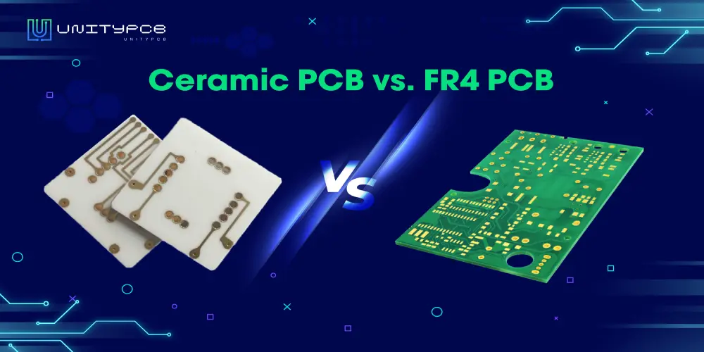
Ceramic PCB vs. FR4 PCB: What Are the Differences?
You can see FR4 PCB in many applications. Is it suitable for your product? Understanding the key differences between ceramic PCB vs. FR4 PCB is essential to choosing the right type for your application. The following is a comparison covering the key aspects of them.
| Aspect | Ceramic PCB | FR4 PCB |
| Substrate Materials | Ceramic materials (AIN, Al₂O₃, BeO ) | Glass fiber reinforced epoxy resin (FR4) |
| Thermal Conductivity | High thermal conductivity, suitable for high power density applications | Lower thermal conductivity, not ideal for high power applications |
| Mechanical Strength | Excellent mechanical strength, suitable for applications requiring robust performance | Good mechanical strength, prone to cracking or warping under stress |
| Electrical Performance | Superior for RF application, low signal loss | Limited electrical performance, suitable for general applications |
| CTE Value | Low CTE, reduces thermal stress in applications with significant temperature variation | Higher CTE, which may lead to greater thermal stress when paired with materials that have a lower |
| Manufacturing Complexity | Complex manufacturing process, requires high-temperature sintering | Standard production process, easier to mass-produce |
| Cost | Higher cost due to materials and complex processing | Lower cost, economical for mass production |
Choosing UnityPCB as Your Trusted Ceramic PCB Manufacturer
When you need high-quality ceramic PCB, UnityPCB is your trusted partner to provide innovative and reliable solutions for your project. As an industry-leading ceramic PCB manufacturer, we are committed to providing you with a one-stop service to meet all your design and production needs. With nearly 20 years of rich experience, we provide you with a variety of high-performance products including alumina ceramic PCBs, aluminum nitride ceramic PCBs, etc. Welcome to get a quote and contact us for more details.