With the electronics industry’s continuous advancement, electronic devices are shrinking in size while gaining higher functions. Thanks to HDI PCB, electronic products can be miniaturized and improved in performance by achieving more interconnections in a smaller space. This article will explore HDI PCB in depth to provide a comprehensive understanding.
What Is an HDI PCB?
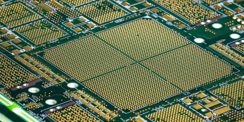
HDI PCB refers to High Density Interconnect Printed Circuit Board with significantly higher routing density than traditional PCB. Its main features include finer traces and spacing (≤0.1mm), smaller microvias (≤0.127mm), and smaller pads (≤0.35mm). Compared with traditional PCB, HDI PCB can achieve the same number of electrical interconnections while reducing the number of layers. It can reduce product weight and improve signal transmission performance at the same time. This kind of PCB is popularly used in electronic products pursuing miniaturization and high performance.
Common Types of High-Density Interconnect Stack-up
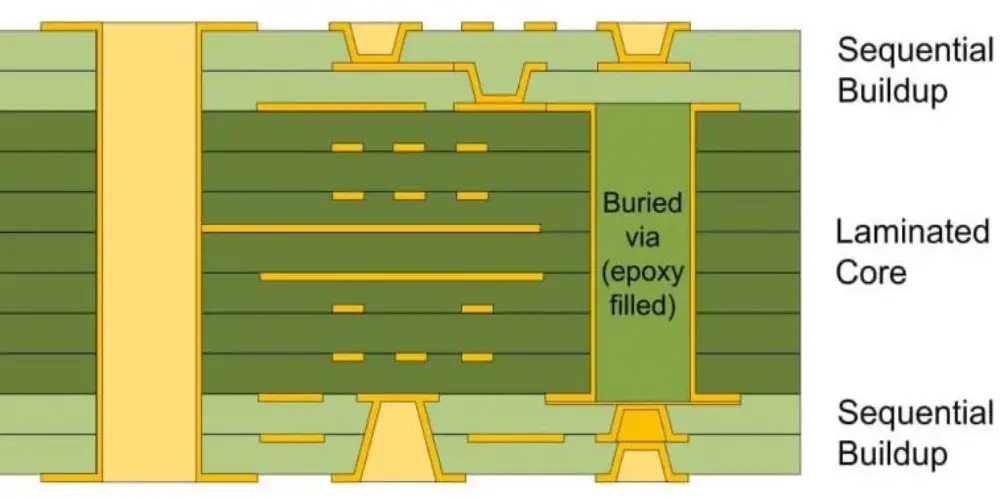
Every layer interconnect (ELIC) and sequential build-up are two common structures of HDI PCB. Sequential build-up is the most popular one. Here we list some common types of HDI PCB stack-up.
HDI PCB (0+N+0): Basic Configuration
This is the simplest stack-up structure. N represents the number of core/base/first lamination. The 0 means no additional HDI sequential build-up layers were added.
HDI PCB (1+N+1): Slightly Complex
The “1” refers to a single sequential lamination on each side of the core, adding two copper layers. This results in a total of N+2 layers. It features fine lines, microvias, and positioning technology to enable a 0.4 mm ball pitch, with outstanding mounting stability and dependability.
HDI PCB (2+N+2): Moderately Complex
The “2” indicates two sequential laminations on each side of the core, adding four copper layers. The total number of layers becomes N+4. This fits for BGAs with higher I/O counts and smaller ball pitches. It can improve routing density in complex designs while keeping thinner completed board thickness.
ELIC: Most Complex
In ELIC structures, every layer of the PCB has high-density interconnection capabilities. Copper-filled stacked microvia technology is used, allowing conductors between any layers to be interconnected. This structure offers reliable electrical connections for highly complex large pin-count devices like CPUs and GPUs in handheld or mobile devices.
Understanding Various Kinds of Vias in HDI Boards
In an HDI circuit board, vias are very tiny conductive holes that interconnect layers, allowing signals to flow between different layers. Due to PCB’s functional requirements, common types of vias include through holes, buried vias, blind vias, and microvias.
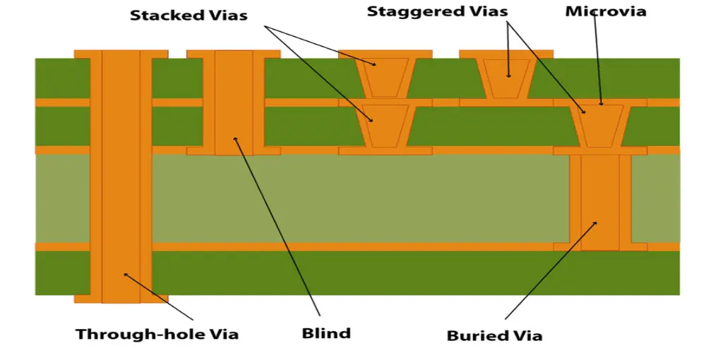
Through-Hole Vias: These vias are through the entire board and can form a conductive path connecting all layers of the board. This kind of via is the most economical. Through holes can be further classified as either non-plated through holes (without copper pads) or plated through holes (with copper pads).
Blind Vias: These are vias that connect the top or bottom layer to one or more inner layers. Unlike through-hole vias, blind vias don’t go through the whole board and are only visible on a single side of the board. This via is difficult to construct and expensive.
Buried Vias: These vias are located inside the printed circuit board and connect two or more inner layers. They cannot be seen from any side of the circuit board, hence the name buried via. This kind of via usually connects even layers, such as 2, 4, or 6, etc. Due to the special location and manufacturing process of the buried via, a separate drill file is required to guide the manufacturing equipment in completing precise processing.
Microvias: These vias are less than 150 microns in diameter and need to be drilled using lasers. Microvias are most commonly found in HDI PCB layout designs and are used to interconnect two adjacent layers. This is the smallest and most space-efficient via type. According to their arrangement, microvias are further divided into the following categories:
- Stacked Vias: Stacked via is a structure consisting of two or more vertically stacked vias that pass through multiple layers of a PCB.
- Staggered Vias: Staggered via achieves inter-layer connection by staggering multiple vias in a non-vertical manner.
- Skip Vias: Skip via is a unique design used to make electrical connections between non-adjacent layers while avoiding going through all intermediate layers.
Key Technologies in HDI PCB Manufacturing
Sequential Lamination and Microvia Drilling
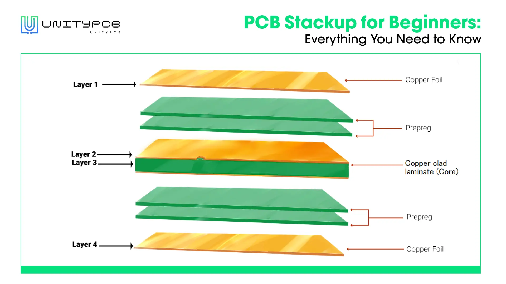
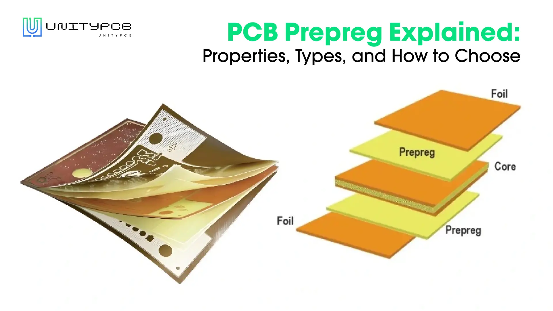
The stacking process is a basic step in HDI PCB manufacturing, which involves two key technologies: microvia drilling and sequential lamination. Microvia drilling creates high-density electrical connections among different layers of a PCB by drilling extremely fine holes. Sequential lamination stacks insulating materials and conductive copper foil layer by layer to build the structure of a multi-layer circuit board.
Copper Plating
There are two main methods of copper plating in HDI PCBs: electrolytic copper plating and electroless copper plating. Electrolytic copper plating is used to provide additional thickness to the conductive layer, enhancing its durability and conductivity. Electroless copper plating is to deposit a thin layer of copper on the surface inside the drilled microvias to ensure the connection between layers.
Useful High Density Interconnect PCB Design Tips
Smart Via Selection
HDI PCBs rely on vias (microvias, blind vias, buried vias) to interconnect layers. The choice of via type directly impacts manufacturing equipment, process complexity, and production steps. Microvias or sequential stacking technology can significantly increase pin density (twice as high as through-holes). Proper via selection is crucial in PCB design to meet performance and functionality requirements.
Optimizing Component Selection
The choice of HDI board components directly affects the routing design, via type, and stack-up structure. HDI boards typically contain SMD (high pin count) and BGA (≤ 0.65 mm) components. Judicious choice of pin pitch can optimize trace width, via type, and stack-up layout, thereby improving overall performance.
Choosing the Right Materials
HDI PCB designs require materials that meet temperature requirements, electrical requirements, and manufacturability. When thinking about the aspect ratio of the microvias that need to be plated, the material’s physical thickness is crucial.
Enhancing Signal Integrity
HDI PCBs use narrower traces, which reduces PCB size. However, the traces need to transmit signals efficiently. The following are some strategies to enhance signal integrity.
- Keep trace lengths as short as possible
- Consistent impedance paths
- Isolate analog,digital, and power signals
- Include adequate ground planes
Why Choose HDI Circuit Boards: Key Advantages Explained
Greater Reliability
HDI PCB board has a smaller aspect ratio design of microvia, which is more reliable than traditional through-hole via. The use of high-quality materials and components makes HDI PCB have excellent performance.
Better Signal Integrity
HDI PCB significantly improves signal integrity by using advanced technologies such as vias in the pad and blind vias. These technologies allow for tighter spacing between components, highly shortening signal transmission paths. HDI technology eliminates via stubs, which also reduces signal reflection and enhances signal integrity.
Compact Size and Lightweight
HDI PCB significantly increases the tracing density per unit area by using a combination of blind vias, buried vias, and microvias, allowing the circuit board to assemble more components in a smaller space. This high-density interconnect design reduces board space requirements as well as enables lighter weight.
Cost-efficient
HDI PCB integrates the functions of multiple standard PCBs into a single circuit board through a highly integrated design, reducing the number of layers and material usage. This design reduces raw material costs and improves overall cost-effectiveness due to HDI PCB’s smaller size, making it more economically advantageous than traditional PCBs.
Typical Applications of HDI Printed Circuit Boards
Consumer Electronics: HDI circuit boards are popularly used in many consumer products due to their compact design. Common applications include smartphones, computers, and wearable devices.
Automotive: Automobiles are getting more computerized and connected. Many advanced devices like GPS, in-car WiFi, backup sensors, and rear-view cameras rely on HDI PCBs.
Aerospace: HDI PCBs can tolerate extreme environmental circumstances. It can be used in defense applications, missile systems, and aircraft.
Medical: HDI PCBs are widely used in advanced equipment in the medical field, both for disease diagnosis and for providing life support. Common devices include pacemakers, miniaturized cameras, and surgical equipment.
Industrial Automation: HDI PCBs are often used in IoT devices and smart sensors in warehousing, manufacturing, and other industrial environments to optimize performance and connectivity. They help companies track equipment, monitor inventory, and optimize operations.
Final Words
HDI PCB has a wide range of applications, covering a variety of fields from consumer electronics to aerospace. As demand for smaller and smarter devices surges, HDI PCB will play a vital role in the future of electronic design and manufacturing. When you are seeking a professional HDI PCB manufacturer, UnityPCB stands out as an excellent choice. With nearly 20 years of experience in PCB manufacturing, UnityPCB offers one-stop services to meet all your PCB needs.
