Product design is a complex and lengthy process. Zero PCB is a type of circuit board widely used in prototyping that has no fixed circuit connections on its surface, allowing users to connect components freely. It provides designers with greater flexibility and freedom, allowing them to quickly transform ideas into operational circuit prototypes. Here we will introduce the key features, advantages, and common applications of zero PCB in detail to help you understand its important role in the design process.
What Is a Zero PCB?
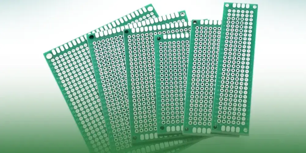
Zero PCB is a general-purpose circuit board, often referred to as Perfboard or Breadboard. It has no predefined circuit connections, layouts, or functions, which makes it extremely flexible. Zero PCB surface has regularly arranged small holes with a hole spacing of 2.54 mm (0.1 inches). Each hole is surrounded by copper pads, and each hole is electrically isolated. Users can insert electronic components into these holes as needed, and connect the components by wires or soldering, without relying on pre-designed copper traces.
Zero PCB is widely used in the prototyping stage and is particularly suitable for rapid testing and modification of circuit designs. It allows engineers and enthusiasts to experiment and verify circuit functions before finalizing the circuit design.
Zero PCB Board Essential Features and Design
Flexibility in Size and Shape
Zero PCB boards can be made into different sizes according to the purpose, from round, rectangular, or square boards to customized shapes according to project requirements. Its design flexibility allows components to be placed arbitrarily, which is convenient for later modification or addition of circuits.
Common zero PCB board sizes include:
| Size | Dimension | Typical Use |
| Small | Around 5×7 cm | Simple projects |
| Medium | Approximately 10×15 cm | Moderate complexity circuits |
| Large | Up to 30×30 cm | Large-scale or extensive projects |
Materials Employed
The materials commonly used in zero PCBs are usually similar to those of standard PCBs. Zero PCBs are mainly made of two materials: FR-2 and FR-4. FR-2 is a paper-based reinforced material. Its electrical and mechanical properties are not as good as FR-4, but it is much cheaper and suitable for low-cost applications. FR-4 is a widely used glass fiber reinforced epoxy resin material with good heat resistance and strong mechanical strength.
Copper Traces, Pads and Holes Design
Zero PCB applies a standard hole spacing of 2.54 mm (0.1 inch), and each hole is surrounded by a copper pad. It provides copper pads and traces, which can be manually connected to create custom circuit paths. Users have the flexibility to insert components into the holes and establish the desired electrical connections through solder wires.
Absence of Solder Mask and Silkscreen Layers
Unlike standard PCB, zero PCB doesn’t have a solder mask and silkscreen layer. Its purpose is to provide users with a completely blank circuit to be able to freely design, place, and solder electronic components without any predefined restrictions.
How to Build Circuits on a Zero Printed Circuit Board?
It is very easy to build a circuit using zero PCB, especially for prototyping. Here are three key steps to help ensure a smooth circuit construction.
Positioning of Components: Component layout on zero PCB boards requires careful planning, and the core goal is to optimize space utilization and circuit performance. An effective layout strategy is to place similar types of components, such as resistors and capacitors, together, which helps reduce wiring clutter and reduces the risk of failure. Before the layout begins, it is recommended to draw a detailed layout diagram to plan the specific location of each component.
Soldering Process: Once the components are positioned, you can begin the soldering process. The soldering process requires a high degree of precision to ensure a stable, error-free connection. Common problems include cold joints and solder bridges between pads. Using flux can improve solder fluidity and ensure a more secure solder connection. Precise operation and skilled soldering techniques are key factors in ensuring soldering quality.
Wire Routing and Connections: When making wiring connections on a zero PCB board, you can use jumper wires or ordinary copper wires to connect the various components. Keeping the wires tidy can not only effectively prevent accidental short circuits, but also simplify future troubleshooting and debugging work.
Zero PCB Vs. Bare PCB: What Are the Differences?
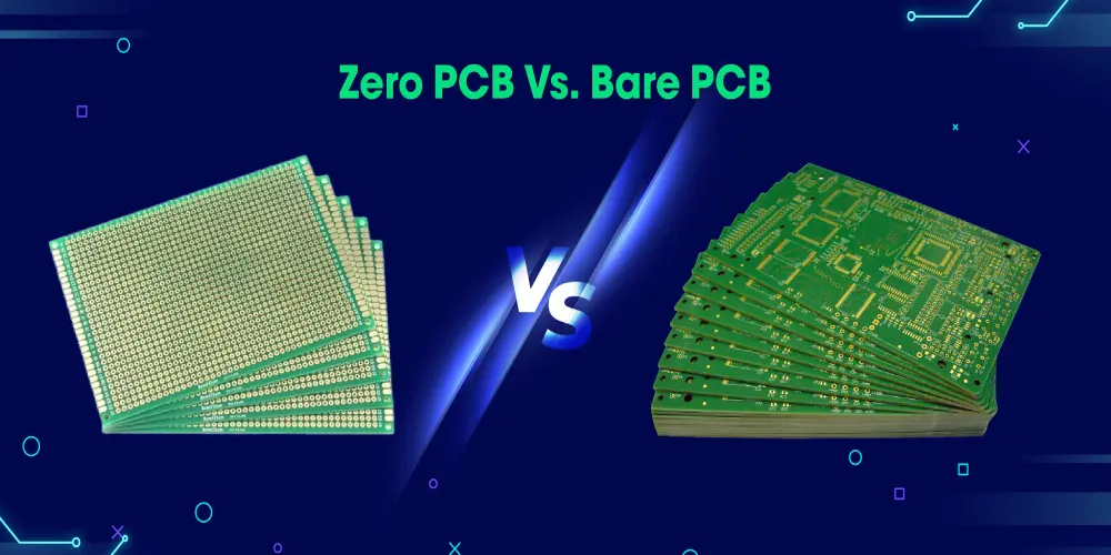
Aspect | Zero PCB | Bare PCB |
| Definition | A generic circuit board without predefined specific functions or designs. | A standard PCB that has not yet been equipped with any electronic components. |
| Manufacturing Process | No solder mask or silkscreen layers. | With copper traces, solder mask, silkscreen, etc. |
| Design Flexibility | Highly flexible and allows quick circuit reconfiguration. | Precisely engineered for specific circuit requirements. |
| Components Assembled | Components can be manually inserted or removed. | Designed for permanent component mounting. |
| Wiring | Requires manual connection of components using wires or jumper cables. | Copper traces are etched directly onto the PCB. |
| Usage | Quick testing, prototyping, and educational purposes. | Used as the foundation for components mounted to be a complete circuit. |
| Cost | Generally low-cost. | Varies based on complexity. |
Typical Benefits of Zero Circuit Boards
Design Flexibility
Zero PCB provides electronic design engineers with significant design freedom, allowing them to quickly and flexibly try and iterate design solutions in the early stages of PCB layout design. It greatly reduces design costs and time investment by easily changing components and adjusting current paths.
Tailored Enclosure Design
With the flexibility of Zero PCB size, we can customize the shape and size of the PCB according to the actual available space to better fit the application environment. In this way, we are able to design the optimal mechanical enclosure in a limited space. Relying only on a tape measure to measure the enclosure size is usually not accurate enough to meet the complex needs of the design.
Early Testing for Functional Validation
Zero PCB has shown significant advantages in early testing. By conducting functional testing on zero PCB, we can identify and analyze potential design defects in advance, such as heat dissipation issues and unreasonable component layouts. This approach reduces repair costs and post-assembly board issues, ensuring design flaws are corrected at an early stage.
Optimized Cost Approach
By using zero printed circuit boards in the early stages, we can effectively reduce expensive redesign, assembly, and testing processes. This approach not only minimizes the risk of damage to high-value components but also comprehensively evaluates the reliability of products in a more economical way.
What Are the Common Applications of Zero PCBs?
Zero PCB has a wide range of applications, with three key areas highlighted in detail below.
Educational Purposes
Zero PCBs play an important role in the field of education. In schools, zero PCBs are a great tool to cultivate students’ interest in electronics, allowing beginners to learn basic circuit design and soldering techniques by connecting LEDs and sensors. It provides a hands-on platform that allows students to gain a deep understanding of electronic design principles in a real environment.
Innovative DIY Projects
Zero PCB has become popular among DIY enthusiasts as an ideal platform for creativity and experimentation. Its low cost and high flexibility make it perfect for a wide range of innovative projects, helping turn ideas into functional circuits.
Fast Prototyping Solutions
Zero PCB provides a low-cost, fast, and flexible solution for prototyping and circuit verification. Designers can quickly troubleshoot and optimize designs by simply soldering and adjusting circuit connections without relying on professional manufacturing, significantly improving design and debugging efficiency.
Choose UnityPCB as Your Trusted Professional Partner
Using zero PCB, designers can significantly reduce design costs and quickly identify and resolve potential issues at an early stage. Zero PCB helps improve the efficiency of design iterations and avoids complex modifications and high rework costs in the future. If you need a PCB prototype design, UnityPCB is your ideal choice. We will help you turn your innovative ideas into reality. With nearly 20 years of industry experience, UnityPCB provides high-quality PCB design, manufacturing, and assembly services. Contact UnityPCB now to learn more about our products and services!