We all know in the electronics industry that precision and reliability are key, especially when it comes to Surface Mount Device (SMD) soldering. However, as our gadgets become more and more smaller and complex, accuracy with the solder paste is paramount to get all of it working seamlessly. That’s where PCB stencils come in — they are the unsung heroes making sure solder paste is placed where it should be without fail.
So, what exactly is a PCB stencil, and why is it crucial? In this blog, we will explore the different types of stencils, their benefits, and application process. Let’s dive in!
What Is a Stencil in PCB?
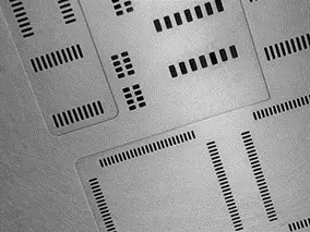
A PCB stencil—also called an SMT stencil—is basically a thin sheet of stainless steel with tiny openings cut into it using a laser. These openings match up perfectly with the spots on your PCB where you need to place solder paste. When you lay the stencil over the board and spread the solder paste through it, it ensures that the paste goes exactly where it’s supposed to go, and nowhere else.
The main job of a SMT stencil is to put just the right amount of solder paste onto the pads where your components will sit. This way, when you place the components on the board, they’ll be perfectly aligned and securely held in place.
Advantages of Using PCB Stencils
- Improved Precision
PCB stencils make sure that the solder paste is placed at the right place on the pads. It decreases errors and eliminates rework.
- Time Efficiency
The process of applying solder paste is accelerated by automated stencil printing. It is highly suitable for mass production environment, where speed is a must.
- Consistent Quality
Circuit board stencils standardize the deposition of solder paste resulting in consistent solder paste application across a batch of units.
- Cost-Effective
The use of SMT stencils reduces manual labor requirements and lowers rework costs. It is a cost-effective option for manufacturers.
3 Commonly Used PCB Stencil Types
PCB stencils can be classified into various types depending on their design and manufacturing method. In this article, we will focus on the most commonly used types:
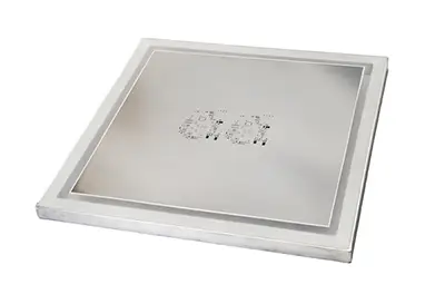
Framed PCB Stencil
Framed PCB stencils are the traditional choice for SMT assembly. These stencils consist of a thin metal sheet with perforations, supported by a rigid metal frame. The frame keeps stencils from moving out of position or warping when applying the solder paste to the stencil. Because of their durability and consistency, framed stencils are very suited to large production runs.
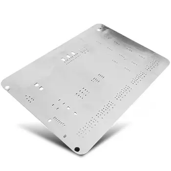
Frameless SMT Stencil
Frameless stencils are stencils that have no frame around the stencil. This design leads to lower costs, so it is more economical. This kind of circuit board stencil can be put on the PCB directly, easy to use, and lightweight. Therefore, they are best suited for hobbyists and non-repetitive use. Additionally, they’re also easier to be shipped and more convenient for smaller batch PCB printing as you can get custom sizes without extra frame support.
Step Stencil
A step stencil has different thickness levels within the same stencil. It’s designed for PCBs with components that need diverse amounts of solder paste. Because of its stepped design, it can apply the right amount of paste to each component, making it ideal for mixed-technology assemblies where components have different sizes and solder requirements.
Step-by-Step Guide: PCB Stencil Application Process
Step 1: Check PCB and Stencil
Make sure that both PCB and stencil are clean and do not have defects. If you find the stencil is dirty, clean it using isopropyl alcohol and lint free wipes. The surface of PCB should also be cleaned without any contamination.
Step 2: Workstation Organization
Set up a clean, well-lit workspace with a flat surface. Have all required tools ready: tweezers, cleaning supplies, PCB fixture, scraper, hot air gun.
Step 3: Stencil and PCB Alignment
Put the PCB in it’s holding fixture and carefully align the stencil with reference marks. Proper alignment is crucial for precise solder paste placement.
Step 4: Solder Paste Application
Apply solder paste to one end of the stencil. Use the scraper in a 45 degree angle, and apply even amount of paste to all the openings with same pressure.
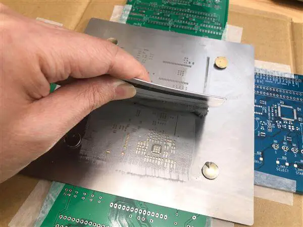
Step 5: Stencil Removal
Start from one corner to carefully lift the stencil vertically. Don’t move any sideways at all as it could smear the paste. Be sure all pads have proper amounts of solder paste coverage.
Considerations When Developing PCB Stencil
When designing or ordering a PCB stencil, it’s important to consider several key factors to achieve the best performance:
Stencil Thickness
The thickness of circuit board stencil is the foremost factor to consider as it directly determines the amount of solder paste that jumps through the openings. An accurate thickness is essential to ensure that the amount of solder paste applied is proper. If there’s too much solder, it will cause bridging, or if there’s too little, the solder joints will be too weak and that would affect functionality of the final PCBA.
Aperture Size
The stencil openings should be designed slightly smaller than the PCB pad size, so as to minimize solder defects such as bridging and solder beads. When applying the solder paste, there is a chance that some paste could end up on the PCB or deposited onto the stencil’s aperture wall. And to prevent this issue, the PCB pad area should always be more than two-thirds of the area inside the stencil aperture wall.
PCB Stencil Material
Stencil performance is highly dependent on the material used for the stencil. Stainless steel is the most common material with its durability and ability to transport solder paste effectively from the aperture to the PCB pad.
Stencil Alignment
Precise solder paste deposition requires exact alignment between the circuit board and stencil. It is suggested to make some fiducial marks on the PCB, and on the stencil. These marks serve to place the stencil accurately over the PCB, and to provide a perfect print of solder paste onto the pads.
How to Clean the PCB stencil?
After using the stencil, once the solder paste has been removed by the screen printing machine operator, it’s important to clean the stencil’s openings and walls thoroughly. After screen printing, if you notice any blockages, clean the stencil right away.
To start, use a special wiping paper that’s been dampened with alcohol to clean the stencil’s surface. Hold the wiping paper with one hand and gently clean the underside of the stencil with the alcohol. Meanwhile, use a soft brush in the other hand to scrub the stencil surface and its openings. Work methodically, cleaning the openings from left side to right side, and from top to bottom.
Key Takeaways
PCB stencils are vital in the process of efficiently and correctly achieving high quality PCB assembly. No matter if you are working on prototypes or on large production runs, it’s important to know how to use and maintain these stencils properly to achieve your desired results. If you require professional PCB assembly services including stencil design and application, UnityPCB is here to help. Reach out to us today to find out more!