Our lives are surrounded by various electronic devices, and when taking them apart, we often find green boards known as PCBs (printed circuit boards). They are used in almost all electronic products and accessories, such as aerospace devices, medical equipment, cell phones, computers, etc. Since PCBs are widely used everywhere, how much do you know about them? This is the ultimate guide for beginners to learn what printed circuit boards are, how they are made, and their common applications.
What Is a PCB? Why Is It Useful?
Printed circuit boards are boards that are made from non-conductive materials with conductive traces etched or printed on the surface of the conductive layer to enable the mounted electronic components to work. The non-conductive layer is usually made of FR4 and polyimide, with insulation, waterproofing, and stability. The conductive layer is generally made of copper with high electrical conductivity.
The invention of PCB helped in addressing the issues of complex, bulky, and fragile circuits. Thus, circuits can be brought together on a circuit board and this makes them compact, efficient, and less susceptible to breakages. PCB manufacturing follows procedures that enable mass production while guaranteeing consistent performance and quality.
The History and Evolution of PCB
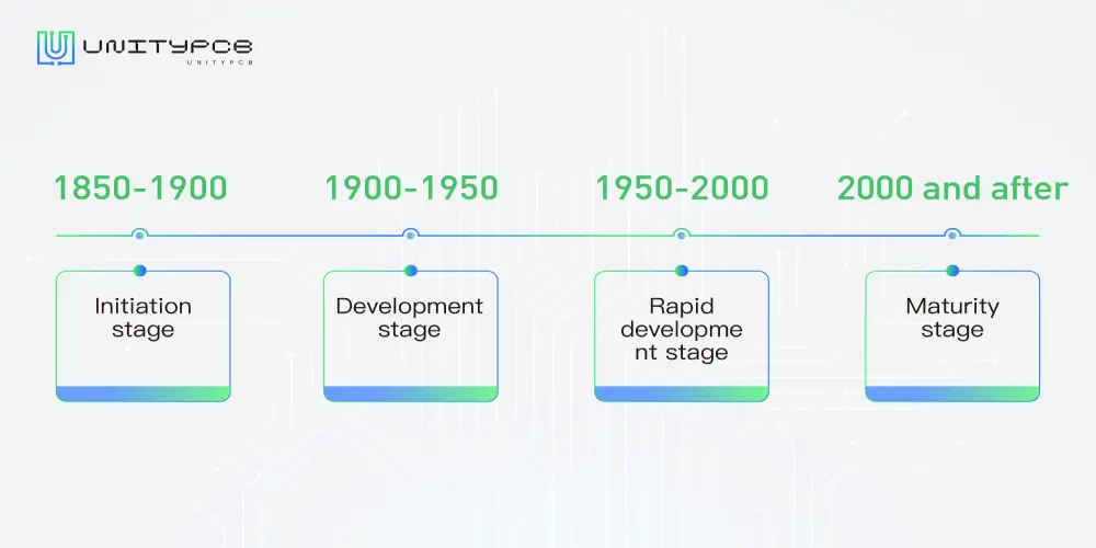
Initiation stage:1850-1900
With the popularization of electricity, the emergence of telephones and light bulbs laid the foundation for the technological development of printed circuit boards.
Development stage:1900-1950
A large number of telephones in the United States required people to change telephone connections. In 1903, Albert Hanson from Germany patented the first PCB-like device for use in telephone systems.
In 1925, Charles Ducas printed a circuit on an insulated substrate and then built up the conductors used for wiring by using electroplating. It means the printed circuit board was truly born.
In 1941, inventor Eisler introduced the concept of printed circuit board, which used copper foil on a non-conductive glass base. It is considered the first modern printed circuit board.
Rapid development stage:1950-2000
Americans desired to explore space after World War II. Printed circuit boards made it possible to explore space. Printed circuit boards are lightweight, consume less power, and are more efficient when performing very complex tasks.
Maturity stage:2000 and after
Since the 2000s, rapid technology advancements have driven the evolution of printed circuit boards. They are becoming more complex, smaller, and lighter, making them widely used in a variety of industries including smart homes, self-driving cars, and artificial intelligence.
4 Fundamental Layers of PCB
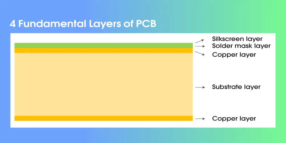
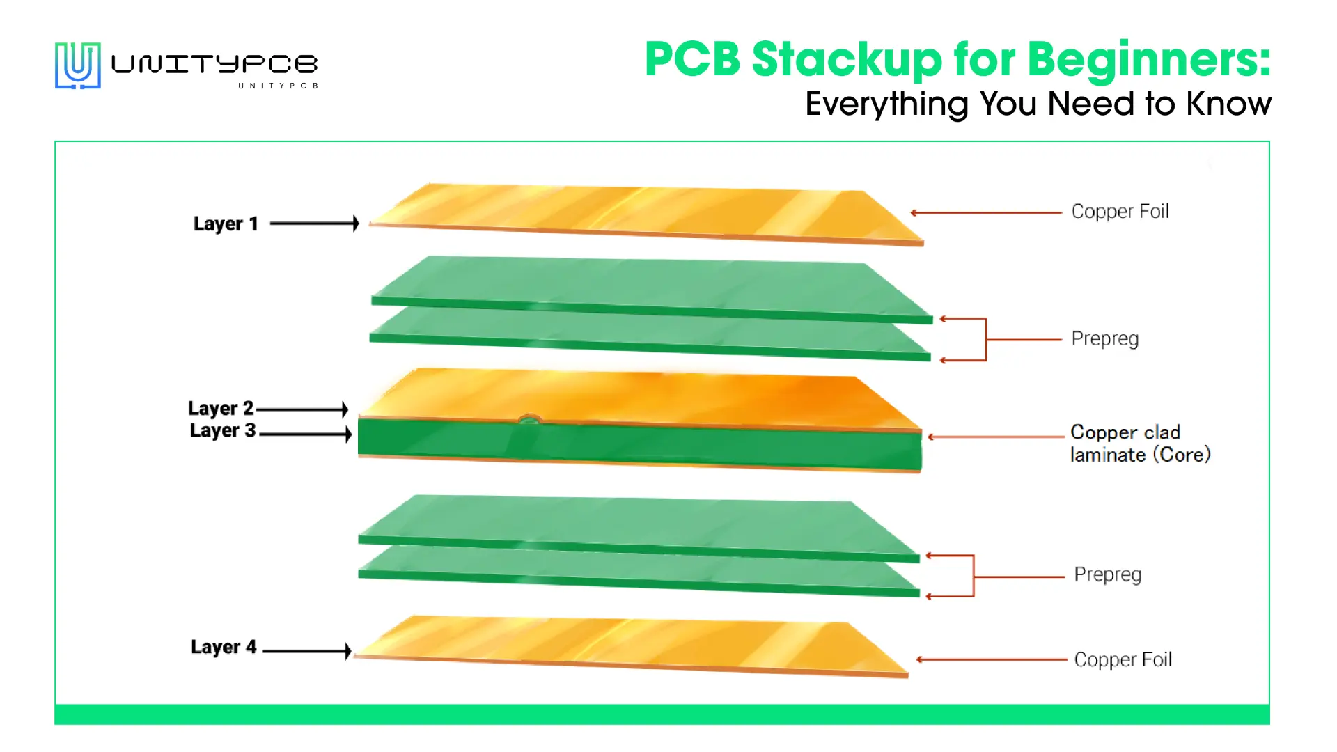
PCB is comprised of at least the following four layers. If PCBs have more functions, more layers are needed.
Substrate layer
The substrate layer is the printed circuit board basic structure, which serves both for insulation and physical strength. It is usually made of FR-4 or some other low-cost insulating rigid material. FR-4 is preferred because of its efficiency and ease of inexpensive mass production. In addition, it is also possible to use flexible type (often plastic) substrates for folding and binding purposes depending on the given use case scenario.
Copper layer
The conductive layer usually refers to a thin copper foil that is bonded to the substrate. In a printed circuit board, the copper layer is a conductive trace, that serves the purpose of electronic signal transmission.
Solder mask layer
Generally, the solder mask layer is non-conductive and is used to coat the PCB which gives the board a green color, other colors are also possible. The solder mask layer is on top of the copper and insulates the copper from touching other elements.
Silkscreen layer
The silkscreen layer is the last layer of the circuit board which can allow letters, numbers, and symbols to be added to the board. It is easy for users to identify and comprehend different features and components on the board.
How Is a PCB Manufactured: Step-by-step Overview
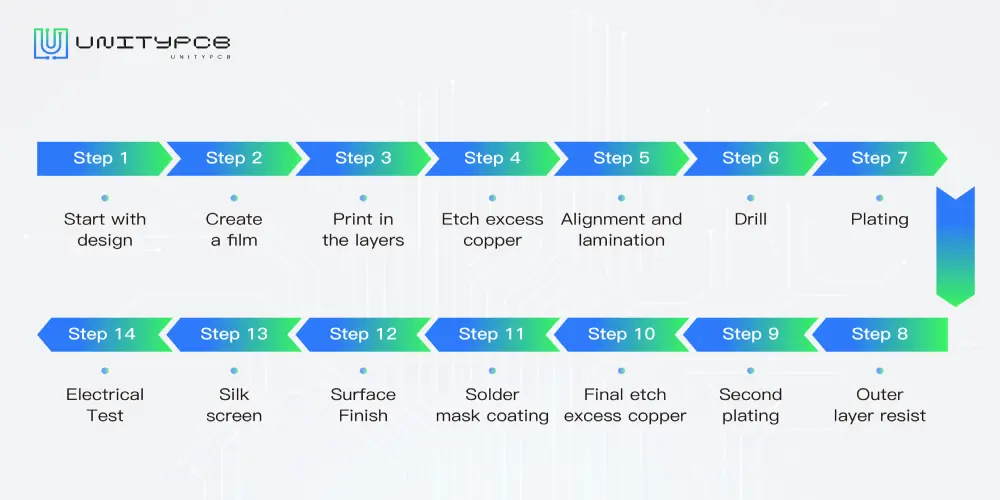
Step 1: Start with design
Designers use PCB design software to design the appearance and functionality of circuit boards, including trace layers, components, and other relevant information.
Step 2: Create a film
Using a special printer, print the PCB design.
Step 3: Print in the layers
In this step, copper layers are bonded to the sides of the substrate, and print the printed circuit board design to a copper layer. Add photosensitive film (photoresist) to the panel.
Step 4: Etch excess copper
The excess copper is etched away with a chemical solution, and the required copper is protected from corrosion with a hardened photoresist.
Step 5: Alignment and lamination
Align and laminate all layers together. From this step on, mistakes in the inner layers cannot be corrected. Therefore, it is important to perform AOI(automated optical inspection) to confirm there are no errors.
Step 6: Drill
Drill holes for plating. It is used to connect components and connect copper layers.
Step 7: Plating
The electroplating process is to fuse different layers of a PCB through chemicals. After thorough cleaning, a thin layer of copper is deposited on the surface during the plating process, and the copper also enters the most recently drilled hole.
Step 8: Outer layer resist
A photoresist is applied to a panel to image the outer layer on a printed circuit board, similar to how the inner layer is imaged.
Step 9: Second plating
A layer of copper plating is also required. Starting with the previous copper plating, a layer of tin is applied to prevent etching away any desired copper.
Step 10: Final etch excess copper
The unwanted copper is removed with a chemical solution, and the tin protects the needed copper at this stage.
Step 11: Solder mask coating
After the board is cleaned, the solder mask is covered on both sides and irradiated with a UV light. Ultraviolet light passes through the soldering mask photo film, and the unhardened part is removed.
Step 12: Surface Finish
Gold or silver plating is applied to circuit boards to prevent the copper pads from oxidation, and provide a smooth surface for soldering components.
Step 13: Silk screen
The circuit board receives inkjet writes on its surface, which is used to indicate relevant information. The PCB finally enters the final coating and curing stage.
Step 14: Electrical Test
Finally, perform electrical testing on the PCB. This is mainly to detect whether the functions of the circuit board can be used normally.
Common Types of Printed Circuit Boards
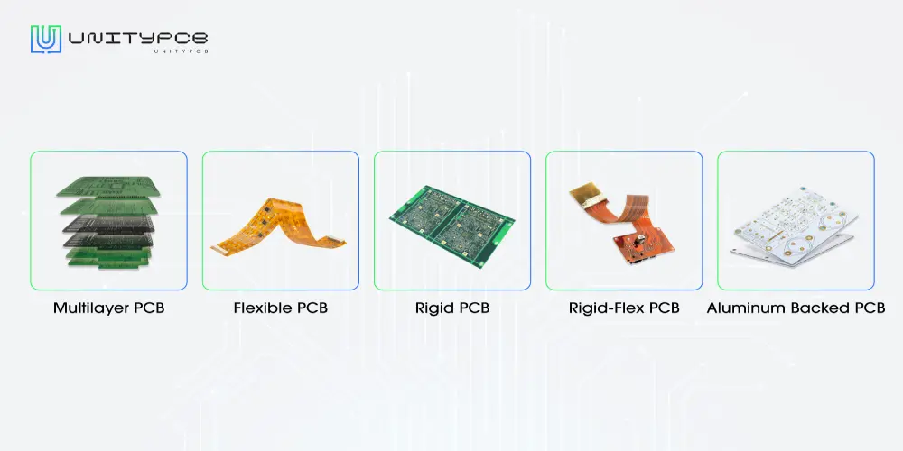
Single-layer PCBs
Single-side PCB, one side is the conductive copper layer, and the other side is for electronic components. This type of printed circuit board is inexpensive, quick to produce, and simple to design.
Double-layer PCBs
A double-sided PCB is a substrate with conductive copper layers on both sides, and the components on both sides are connected through holes. It has broader applications and can implement more sophisticated circuits. It works well with advanced electronic systems.
Multilayer PCBs
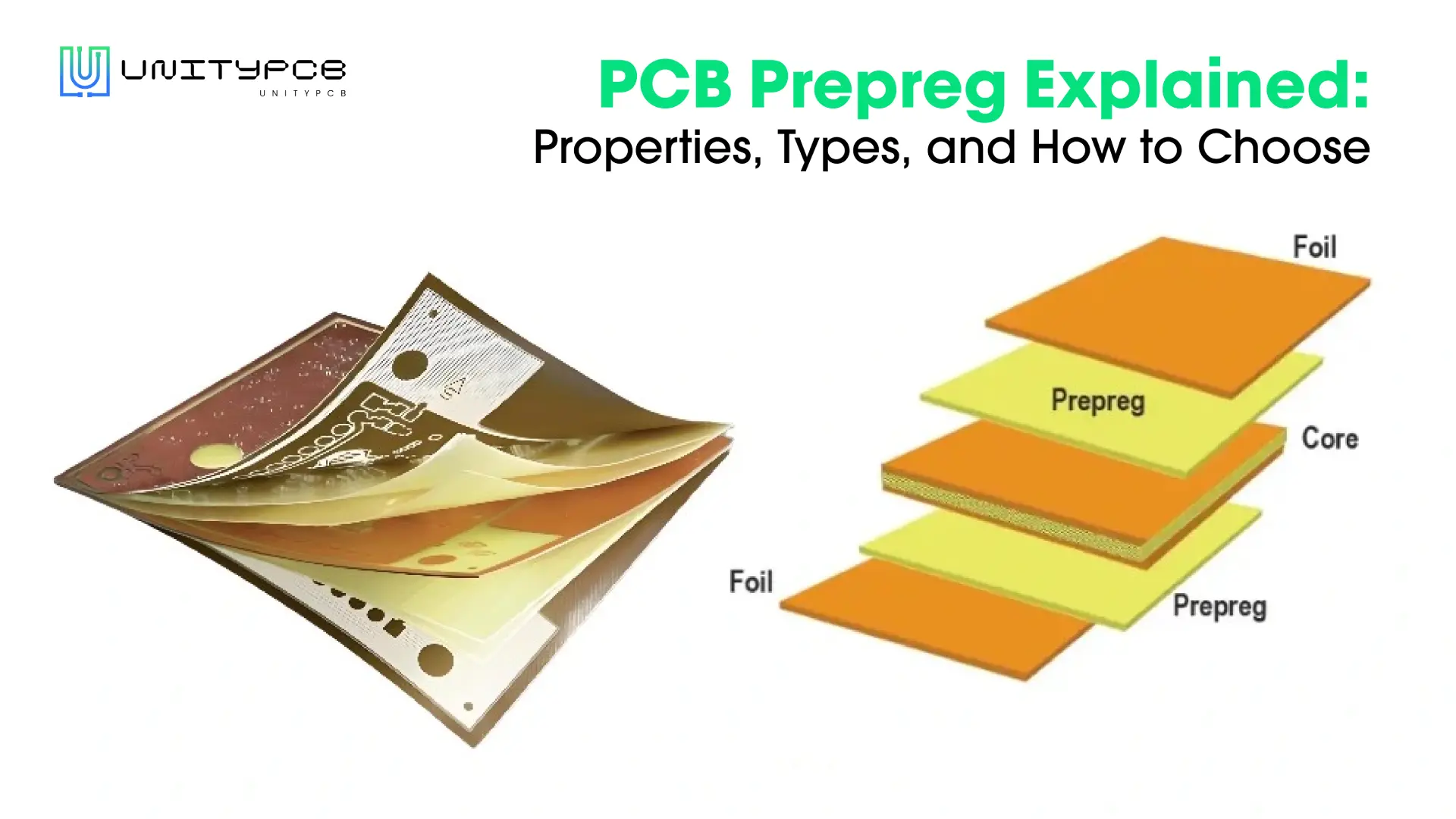
Multilayer PCBs are made up of three or more conductive layers separated by a corresponding number of substrates and then laminated together. Since Multilayer PCBs have more layers, they can serve more components and complex circuits in a smaller area. Due to its excellent performance, it is popularly used in aerospace systems, defense systems, and medical devices.
Flexible PCBs
The substrate of Flex PCBs is flexible, usually polyamide, and can be single, double, or even multilayer. The advantage of Flex printed circuit boards is that they can be bent to the desired form without damaging the wires and can save space. These boards are suitable for irregularly shaped or vibration-resistant applications such as wearable electronics.
Rigid PCBs
The substrates of Rigid PCBs are non-bendable, foldable, and can be single, double, or multi-layer. These boards cannot be modified after they have been manufactured. They are cost-effective and are more durable than other circuit boards. It’s easy to repair and maintain. Rigid PCBs are commonly used in everyday products such as computers and cell phones, as well as large non-portable medical devices.
Rigid-Flex PCBs
Rigid-Flex PCB has advantages of both the rigid circuit board and flexible circuit board. It is not only flexible but also sturdy, allowing the formation of folded or continuously bent circuits. They achieve higher spatial performance through 3D design, which can be used in situations where there are special requirements for space and weight, especially in the medical and aerospace fields.
Aluminum Backed PCBs
Aluminum-backed PCBs consist of a metal base and copper foil-covered laminate. They are suitable for high-power applications where the aluminum construction helps dissipate heat and cool the electronic components.
Things Need to Consider When Choosing a PCB
Since there are numerous kinds of PCBs, how do we make the proper selection? The following aspects are the crucial points to consider when selecting suitable printed circuit boards.
Materials
PCB boards are usually made of FR4 (glass-reinforced epoxy resin) because of good insulation and durability. If the boards have special requirements, other substrates can be selected.
Layers
Single-layer boards carry fewer assemblies, double-sided boards allow more components, and multilayers are used for complex electronic circuits.
Size
The size of the board depends on the size of the device, there is enough space for all the components without being too crowded.
Cost consideration
When we choose materials, cost is an important aspect to evaluate. Factors like design complexity, number of layers, and specialty materials all affect price.
Top 6 Applications of PCB
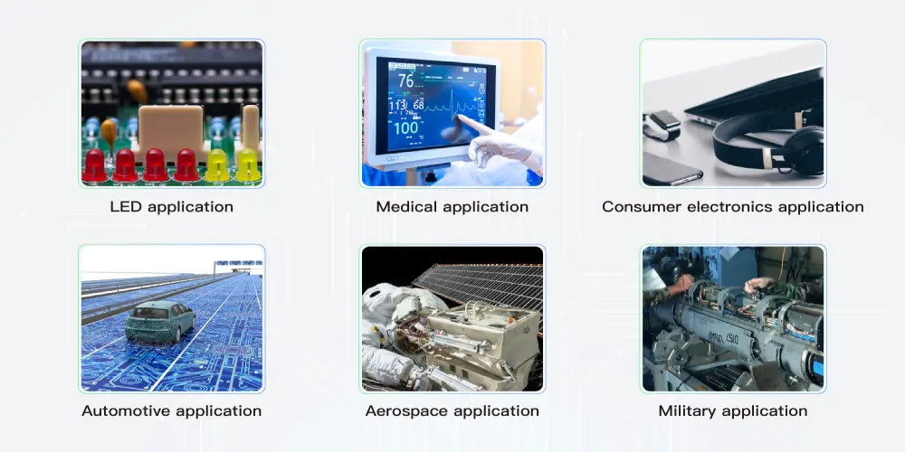
PCB has a very large scale of application in many industries and areas. Here we mainly introduce 6 common applications:
LED application
LEDs are an important type of lighting because of their compact size, long lifespan, and high energy efficiency. PCBs and LED technology work together to transfer heat away from the bulb and increase the life of the LED. Printed circuit boards used in LEDs, usually made of aluminum, have strong thermal conductivity.
Medical application
With the advancement of PCB technology, more and more circuit boards are being used in the medical industry. Printed circuit boards are important components in devices used for diagnosis, monitoring, treatment, and more. In medical applications, these are health-related products that need to meet requirements for repeatability and reliability.
Consumer electronics application
The products we use frequently in our daily lives, such as mobile phones, computers, home appliances, and other consumer electronics, all require the support of printed circuit boards to function properly. More and more printed circuit boards are added to products, and our daily life is also inseparable from them.
Automotive application
In the past, printed circuit boards were only used for headlight switches and windshield wipers in automobiles. Now, automakers are using more and more electronic components in the cars, such as entertainment and navigation systems, control systems, and sensors.
Aerospace application
The aerospace industry also uses a large number of printed circuit boards, but the materials used to manufacture circuit boards need to be able to withstand vibrations, extreme temperatures, and other harsh environments. These printed circuit boards are commonly used in power supplies, monitoring devices, and communication equipment.
Military application
The military makes extensive use of printed circuit boards, which you can find in communication equipment, computers, vehicles, and firearms. The military is often at the forefront of technology, and some of the most advanced uses of printed circuit boards are also for military and defense applications.
The Latest Trends in Printed Circuit Board Manufacturing
3D printing
A new trend in printed circuit board manufacturing is the use of 3D printing. It can produce the high complex circuit boards with little waste, time, and cost as compared to the other methods. 3D printing reduces the time it takes to complete the manufacturing of products so that products are taken to the market sooner. It is also a desirable solution for customized mass production of PCBs.
Artificial intelligence (AI)
AI has gradually developed in all walks of life. In PCB manufacturing, AI can help improve quality and shorten production time, increasing the degree of automation in manufacturing. Manufacturers can use AI to analyze data at every step of the process and optimize the entire process.
IoT in PCBs
The development of the Internet of Things has also further promoted the development of the printed circuit board industry. Manufacturers have been designing smaller, more powerful circuit boards to fit smaller products. These products are smaller, more flexible, and at the same time offer higher performance.
Sustainable development
With the global push for green manufacturing, sustainable printed circuit board manufacturing is a key point for the future of manufacturing. Some of the conventional materials that are used in circuit board manufacturing include metals and chemicals that are hazardous to the environment and are not easily recycled. Research and innovation in recyclable materials for PCB manufacturing is a key innovation point for the future.
Conclusion
PCBs are made up of conductive copper routes etched on an insulating substrate. They have evolved over the years and now the boards are complex and high-performance. They are suitable for different high-tech electronic devices. Thus, advanced circuit boards can push the development of the electronic industry. In the future, PCBs also need to follow up the technological developments and update them accordingly.
