Multilayer PCBs (Printed Circuit Boards) have come to be an integral part of the world we live in, which can be found in almost all electronic devices. These sophisticated circuit boards consist of multiple layers of conductive patterns for superior functionality in compact space – a crucial advancement from traditional single and double sided boards. As electronic devices are becoming increasingly complex while shrinking in size, it is essential for engineers and manufacturers to understand multilayer PCB technology. In this detailed guide, we will explore everything you need to know about this key technology of modern electronics.
What Is a Multilayer PCB?
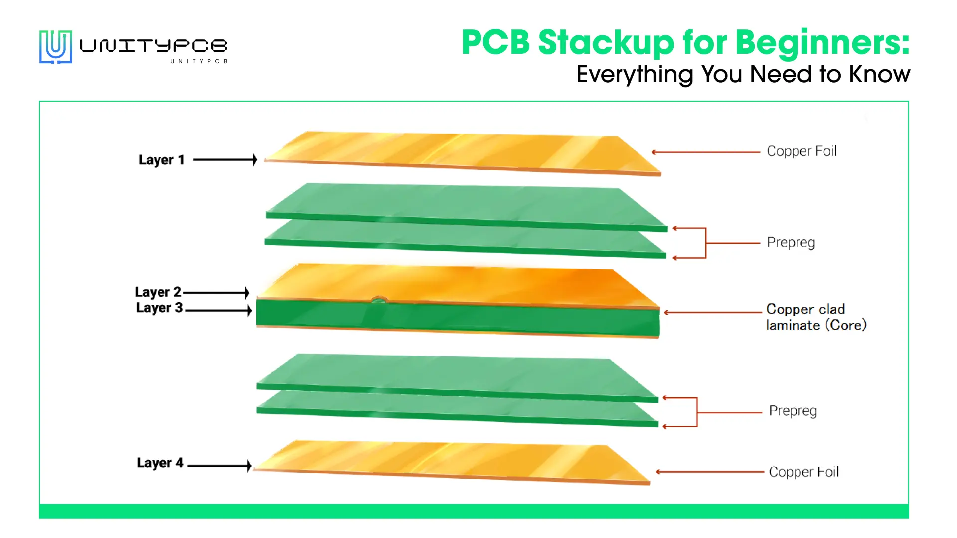
A multilayer PCB refers to a printed circuit board with more than two conductive layers. Inside, multiple layers of copper foil are separated by insulating material (prepreg) and bonded together under pressure to create a solid and single board. This smart layering technique lets engineers pack complex circuits into a smaller space, making electronic devices more powerful and efficient.
Most multilayer PCBs range from 4 to 12 layers, though some advanced applications need even more. With each additional layer providing more routing space, these boards can support sophisticated circuitry and higher component density – a must-have for today’s electronic devices.
What’s the Difference between Multilayer PCB and Single Layer PCB?
A single-layer PCB has just 1 copper layer with components mounted on one side. It’s straightforward to produce and cost-effective, perfect for simple electronics where space isn’t tight. Multilayer PCBs, on the other hand, stack multiple copper layers with insulating materials between them. This design lets them handle complex circuits in a compact space where every millimeter counts.
To identify if a board is single layer or multiple layer, we can hold the board up to a light source. If you see a dark, opaque core, you’re looking at a multilayer board. A transparent core means it’s single or double-sided. Single-layer boards are easiest to spot – their holes won’t have any copper inside.
Understanding Multilayer PCB Stackup Structure
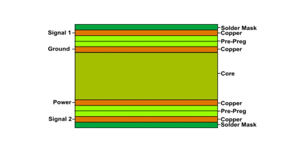
Multilayer PCB stackup engineering is a complex and meticulous way in which circuit boards are built. Typically, the FR-4 is used as the base material, which is copper clad on both sides of it and other layers are built up based on a prepregnated material and a copper foil.
The design of the board also has a symmetric layout to avoid board warping during the manufacturing process and during thermal cycling. Each layer serves a specific purpose: The outer layers mount components and control signal flow, and the inner layers serve as power and ground planes. To retain signals, and minimize the effects of electromagnetic interference, critical signal layers are laid close to ground planes. Each layer is calculated to such thickness so as to satisfy certain electrical requirements. The high pressure and high temperature lamination process forms a unified circuit board in a single complete stack up. It is this method that allows each layer to become systematic and effectively perform complex electronic communications.
Advatanges of Multilayer PCB
- Smaller Size: Multilayer PCBs save a lot of space since instead of making multiple connected circuits horizontally, they are made vertically. They can contain more components and yet the size is still small, making them suitable for today’s portable electronics and applications with limited board space.
- Improved Signal Integrity: Another benefit is that these boards provide better signal separation and shorter trace lengths. Power and ground planes can be placed between signal layers to minimize electromagnetic interference and crosstalk. This architecture provides cleaner signal transmission and supports for high speed applications.
- Enhanced Reliability: Multilayer PCB offers improved heat dissipation and environmental protection for the internal layers of the board. Low noise and stable power distribution are enabled by dedicated power and ground planes, and internal traces are shielded from mechanical stress and contamination.
- Design Flexibility: Engineers get a lot of freedom in terms of routing and component placement on multiple layers. This enables designers to utilize signal paths, distribute power and realize complex circuits with relative ease.
Disadvantages of Multilayer PCB
- Higher Cost: The manufacturing process of multilayer PCB is complex, which involves using specialized equipment, precise lamination, drilling, and additional materials. Thus, the cost of fabricating a multilayer circuit board would be increased.
- More Complicated Design: Compared to single or double-layer PCBs, designing a multilayer PCB board is more complicated. This process requires sophisticated design tools and expertise. Engineers must carefully consider layer stackup, via placement, and impedance control.
- Longer Lead Times: The production times are long leading from an additional quality control steps and more intricate testing requirements associated with the complex manufacturing process. For high volume production runs, or when quick modifications are required, this can affect project schedule and time to market.
How Multilayer PCBs Are Made?
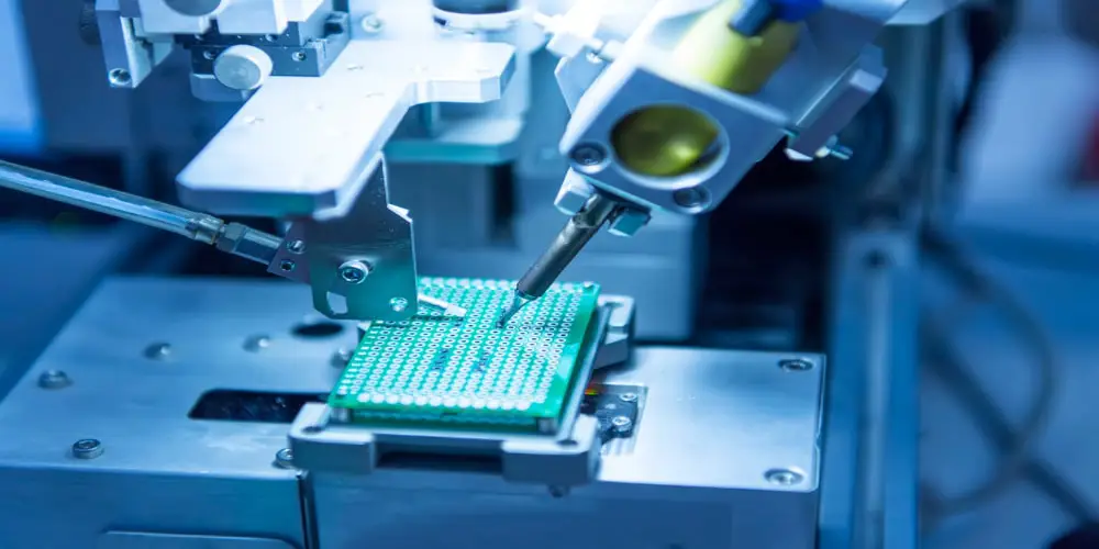
The production of multilayer PCBs includes several crucial steps, Below is an overview of the basic steps:
- Layer Preparation
The process begins with the preparation of copper foil, prepreg (resin-impregnated fiberglass), and core materials like FR4. These layers are stacked and aligned to form the foundation of the PCB. The prepreg provides insulation and mechanical support between the layers.
- Circuit Patterning and Etching
Next, the inner layers are coated with a photosensitive film. The circuit pattern is transferred using UV light, and unexposed areas are etched away, leaving behind the copper traces that form the electrical paths.
- Layer Lamination
The prepared layers are carefully aligned and placed in a lamination press, where heat and pressure are applied to bond the layers together. This step ensures the different layers adhere firmly, forming the multilayer structure.
- Drilling and Plating
In this step, drilling small holes to create vias (electrical connections between layers). These holes are then electroplated with copper to ensure electrical continuity across the layers.
- Outer Layer Imaging and Etching
The outer layers are patterned similarly to the inner layers, with unwanted copper removed through etching. This creates the final traces and pads for components.
- Surface Protection and Marking
A solder mask is applied to protect the PCB and prevent oxidation, followed by silkscreen printing for component markings.
- Testing
A series of tests, such as electrical testing and X-ray inspection, is performed to verify the functionality and reliability of the multilayer PCB before it is shipped out for assembly.
Further reading: How to Test PCB? 7 PCB Testing Methods You Should Know
Common Multilayer PCB Applications
Multilayer PCBs are used in a wide variety of industries, below we list some common applications including:
Consumer Electronics:We can find multilayer PCBs in smartphones, tablets, laptops, and other portable consumer devices that have requirements for compact design and high functionality.
Medical Devices: Multilayer printed circuit boards are essential in medical equipment like diagnostic devices, pacemakers, and monitoring systems, where reliability and miniaturization are critical.
Automotive Electronics: Modern vehicles use multi layer PCB boards for advanced electronics like navigation systems, safety features, and infotainment.
Communication Equipment: Routers, switches, and communication modules utilize multilayer PCBs to handle high-speed data transmission and connectivity.
Industrial Control Systems: Robotics, automation systems, and control boards in industrial machinery often incorporate multilayer PCBs to support complex circuitry and rugged performance.
Get High-quality Mulilayer Circuit Boards from UnityPCB
At UnityPCB, we manufacture the high quality multilayer PCBs up to 18 layers, with capabilities of up to 18 layers, designed to meet the demanding standards of modern electronics. With our advanced facilities and expert engineering team, we ensure precision, reliability and efficiency in every PCB we produce. If you are looking for a trusted multilayer PCB manufacturer, look no further—UnityPCB is your ideal partner. Contact us today to get a free but professional consultation for your projects!
