The soldering process is crucial to the overall quality and performance of a circuit board. The two most commonly used soldering methods are wave soldering vs reflow soldering. These two soldering technologies differ greatly from one another, but do you know when to use which one? Read the following blog, you will learn more about wave soldering vs reflow soldering and their key differences.
What Is Reflow Soldering?
This soldering technology is commonly used for soldering surface mount components on PCBs. In the reflow oven, hot air flow is used to gradually melt and flow the solder paste, forming a firm electrical connection between the component pins and the pads.
How to Execute Reflow Soldering: A Step-by-Step Overview
Before reflow soldering is carried out, these two steps need to be done.
- Apply solder paste to the PCB board using a solder paste stencil.
- The components are precisely put on the pads.
Then through the following steps, the components will be soldered on the circuit board. Here we will explain the key process step by step.
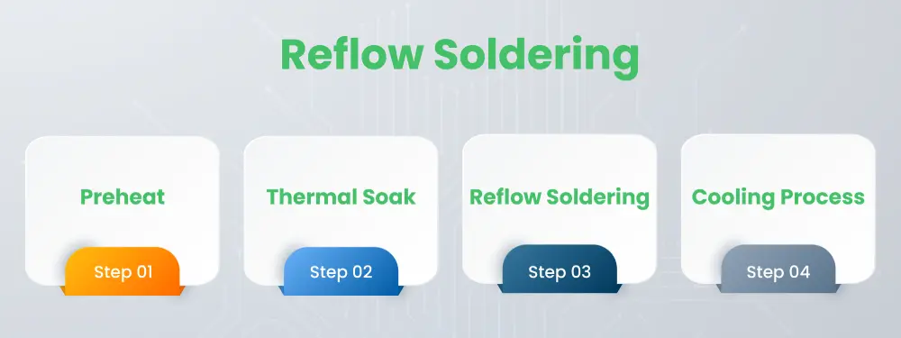
Step 1: Preheat
The preheating step has two main functions in the reflow process:
- By fully preheating PCB and components, damage caused by thermal shock can be effectively prevented, ensuring that they can easily reach the temperature required for soldering
- Preheating can activate the flux and help remove volatile solvents and volatiles in the solder paste, which may affect soldering reliability.
Step 2: Thermal Soak
After completing the preheating, enter the heat-soaking stage. At this stage, the board needs to be kept at an optimal temperature for a period of time, ensuring that every part of the board reaches the correct temperature. Second, the flux must be fully activated, which improves wetting between solder and metal.
Step 3: Reflow Soldering
This is the hottest stage in the soldering process when the solder melts and reflows to form a strong solder joint. Temperature control is key to soldering quality: too low will result in insufficient solder reflow, and too high may damage the board or components.
Step 4: Cooling Process
Once the temperature reaches its peak and begins to drop, the solder paste solidifies, forming a solder joint that firmly fixes the component to the pad on the circuit board.
Typical Reflow Soldering Defects and How to Improve
Solder balls and solder bridges are common reflow soldering defects.
Solder Ball Causes in Reflow Soldering
- Excessive or insufficient temperature can affect solder fluidity. A temperature that’s too high can cause excessive flow, leading to solder balls, while a temperature that’s too low can prevent full melting, resulting in uneven joints and solder balls.
- Inaccurate stencil etching may result in poor solder paste formation, burrs, or indentations, which may form solder balls during the soldering.
- The PCB is not clean enough and there is residual solder. After high-temperature reflow, the residual solder may be scattered around the pad to form solder balls.
How to Reduce Solder Ball Formation?
- Control the preheating temperature and reasonably adjust the reflow soldering temperature curve to reduce the formation of tin ball
- Redesign the solder joint pattern and spacing, and adjust the printing parameters and pressure to improve the printing quality.
- Clean the second-printed PCB to remove residual solder paste.
Solder Bridge Causes in Reflow Soldering
- Solder specification and quality issues lead to reduced solder fluidity and the formation of solder bridges.
- The opening size of the Solder Stencil is too large or the printing pressure is too high, resulting in excessive solder paste or collapse of the formation, forming solder bridges.
- The reflow process heats up too quickly or lasts too long, causing the solder components in the solder paste to evaporate quickly, forming solder bridges.
How to Reduce Solder Bridge Formation?
- Select solder of appropriate specifications and quality, and standardize its application and storage.
- Select the appropriate steel stencil opening size and printing pressure to ensure the cleanliness of solder paste printing and prevent solder cracking.
- Control the heating speed and duration to reduce the evaporation of solder components in the solder paste and reduce the formation of solder bridges.
What Is Wave Soldering?
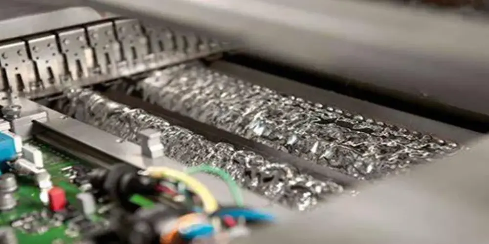
It is a batch soldering technology. A PCB with pre-installed components is quickly conveyed through a wave of molten solder (usually a lead-tin alloy) to solder electronic components. This automated process uses an electric pump to generate a continuous wave of molten soldering material, ensuring a reliable electrical and mechanical connection between the component pins or leads and the PCB pads in seconds. It’s commonly used to soldering through hole components.
How to Conduct Wave Soldering: A Step–by–Step Guide
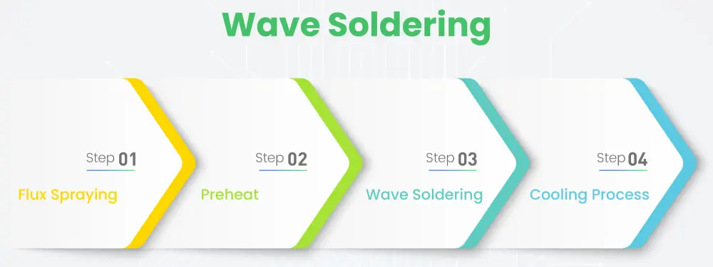
Step 1: Flux Spraying
The flux is sprayed on the bottom of the PCB where soldering is required. Its main functions are:
- Cleaning the PCBmetal surface and component pins to prevent the oxide layer from forming.
- Preventing the formation of oxides during soldering.
- Improving thermal conductivity and helping components to solder.
- Providing lower surface tension
Step 2: Preheat
The PCB passes through a hot tunnel along a chain similar to a conveyor belt. This process preheats the PCB to the appropriate temperature for soldering and activates the flux.
Step 3: Wave Soldering
The solder paste melts into liquid solder and creates a solder wave as the temperature rises. The PCB passes over the solder pad, washed in the wave, and the molten metal alloy adheres to the pins and pads, creating a strong connection.
Step 4: Cooling Process
During the cooling process, the temperature slowly decreases and the solder joints solidify and form a strong connection. The speed of cooling affects the quality of the components, solder joints, and PCBs. At slower cooling rates, components and PCBs can be damaged by overheating. At faster cooling rates, the solder joints may deform, affecting the reliability of the solder joints.
Common Defects of Wave Soldering and How to Improve
Pins Not Connected: The component pins are not in contact with the plug-in holes of the PCB board, resulting in circuit connection failure.
Short Circuit: Solder incorrectly connects the adjacent pins and pads, leading to a short circuit in the circuit.
Voids: Large voids are formed in the plug-in holes or on the surface of the solder joints during the soldering process.
How to Reduce Wave Soldering Defects?
- To solve the problem of no pins, it is necessary to ensure that the wave soldering conveyor chain is flat and use AOI technology to perform soldering quality inspection.
- Optimizing pad spacing and keeping component lead length within the optimal range can effectively reduce short-circuit soldering defects.
- To reduce solder voids, it is necessary to regularly clean the tin slag in the wave soldering oven, ensure uniform application of flux, and accurately control the preheating and soldering temperatures.
Selective Wave Soldering: A Flexible Solution
Both selective wave soldering and wave soldering operate on a similar principle. It enables precise soldering by spraying flux on specific areas that require soldering and using a tray to isolate non-soldering areas from the wave.
Wave Soldering vs Reflow Soldering: Key Pros and Cons Explained
| Parameter | Reflow Soldering | Wave Soldering |
| Pros | ▪ Ideal for SMT assembly. ▪ Can be applied to specific parts of PCB with less waste. ▪ Compact and dense PCB can be achieved. ▪ More material- and energy-efficient in certain production scenarios compared to wave soldering. ▪ Minimizes the risk of solder bridging. ▪ Components avoid direct immersion; thermal shock is minimized. ▪ Multiple solder alloy options including lead-free materials.
| ▪ Ideal for THT assembly. ▪ Soldering speed is fast, reducing the risk of board damage. ▪ Multiple components can be soldered at one time. ▪ Forming reliable joints. ▪ Furnace molten solder circulation ensures uniform composition. ▪ Suitable for high-volume production. ▪ Cost-effective approach.
|
| Cons | ▪ Not suitable for solder THT components. ▪ Need a high-precious stencil to apply solder paste. ▪ High cost of small-scale production. ▪ Various factors can affect soldering quality, such as component size, warpage, PCB layout, insufficient heat dissipation, etc. ▪ High temperatures during reflow soldering can damage sensitive electronic components. | ▪ Difficult to access certain areas of the PCB, limiting precision for delicate components. ▪ Solder bridging may occur, causing a short circuit. ▪ Thermal stress can damage sensitive components. ▪ Molten solder contacts component leads and then reflows in the tank, potentially causing metal contamination of the solder. ▪ Need to cut off the extra pins of the THT components. |
Wave Soldering vs Reflow Soldering: Understanding Key Differences
There are numerous key distinctions between these two techniques: wave soldering vs reflow soldering. We will examine each of them individually below and provide a table for a clear comparison.
Flux Application Differences
Both wave soldering vs reflow soldering require the application of flux, but the methods are different.
- In wave soldering, flux is indeed sprayed first. The main goalof flux is to eliminate the oxide layer on the metal surface. It also cleans the metal surface to ensure that good electrical and mechanical connections can be formed between metals during soldering.
- In reflow soldering, flux is a component of solder paste. During the reflow process, the flux is activated when heated, helping to remove the oxide layer on the pads and component pins, and promoting the flow and wetting of solder.
Manufacturing Efficiency
- Wave soldering is a batch soldering technology that can solder multiple PCBs at the same time. High quality and consistent soldering quality can be achieved by setting and optimizing wave soldering parameters such as wave height, preheating temperature, etc.
- Reflow soldering is soldering one PCB at a time and is a sequential process. Of course, online and continuous reflow ovens can be used to improve efficiency.
Moreover, the production time of wave soldering vs reflow soldering is also affected by other factors such as production volume and product complexity.
Key Equipment and Initial Setup Costs
- Wave soldering requires specialized equipment such as a wave soldering machine and solder cans. Depending on how advanced the equipment is, the cost of a wave soldering machine ranges from $20,000 to $100,000.
- Reflow soldering requires key equipment such as a reflow oven and a stencil printer. Depending on the sophisticated features of the apparatus, reflow ovens can cost anywhere between $50,000 and $300,000.
Here is a table to give a more detailed comparison of wave soldering vs reflow soldering.
| Aspect | Reflow Soldering | Wave Soldering |
| Core Soldering Process | Using hot air to melt the solder and form connections. | Passing the PCB over a molten solder wave to form reliable connections. |
| Production Volume | Can be used for soldering of lower volume production of circuit boards. | Used for batch soldering, it allows for quick, large-scale production. |
| Technique Complexity | It is a relatively uncomplicated technique. | More complex than reflow technology. |
| Soldering Speed | Reflow soldering technology is slower than wave soldering. | Wave soldering takes less time to solder PCB. |
| Defects | Solder ball, Solder bridge | No Pins, Short circuit, Voids |
| Components Compatibility | Surface mount components (SMT) | Through hole components (THT) |
| Lead-Free Compatibility | By adjusting the soldering temperature profile, lead-free solder can be successfully adapted. | Generally demand higher soldering temperatures than lead-based solders. |
| Application | Widely used in surface mount technology (SMT), especially in the production of computers, smartphones, and other consumer electronics. | Usually used in through-hole technology (THT) assembly, especially for switches, connectors, and other large electronic components. |
| Energy Efficiency | Typically more energy-efficient, as heating is localized to the soldering area. | Less energy-efficient due to the requirement of maintaining a large molten solder reservoir. |
| Thermal Stress on Components | Lower thermal stress due to precise control over the heating profile. | Higher thermal stress as the entire PCB is exposed to molten solder. |
Choosing the Right Method for Your PCB Assembly
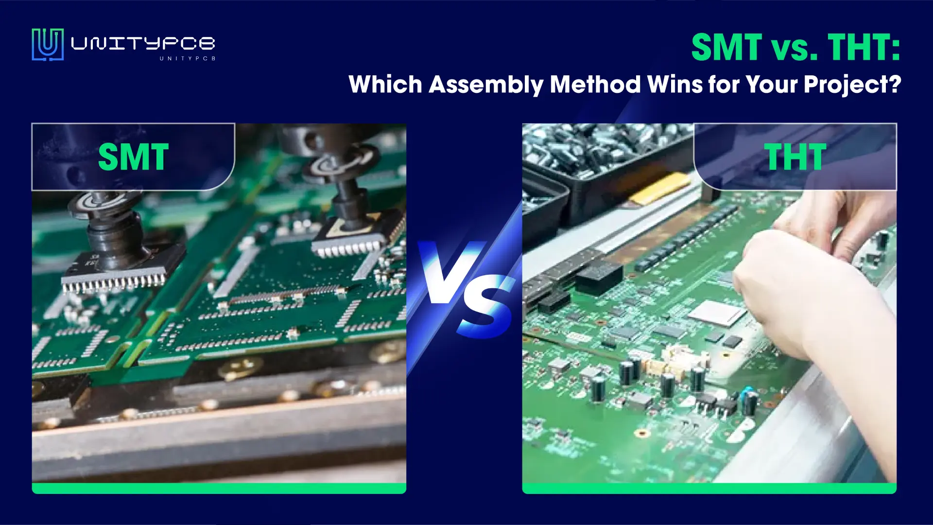
Surface mount components usually use reflow soldering, which allows for soldering some small and delicate components like microchips. While through-hole components are more suitable for wave soldering, providing a strong connection. For PCBs that contain both SMT and THT components, a hybrid soldering solution is the ideal choice. Wave soldering vs reflow soldering have their own advantages and limitations. You need to decide the most suitable soldering process based on factors such as PCB layout design, project budget, production volume, etc.
If you still have questions, please feel free to contact us for professional advice. UnityPCB provides one-stop services including PCB design, manufacturing, and assembly, with advanced facilities to ensure that each PCBA meets high-quality standards. Whether it is prototype design or mass production, we can meet your unique needs.
