PCB silkscreen is often an overlooked part of the PCB manufacturing process. People tend to pay more attention to the technical aspects of PCB design and manufacturing, such as layer stack-up, trace width, and component placement. In fact, these markings may look like simple decorations, but they actually play an essential role in identifying components, guiding assembly, and enhancing the overall usability and aesthetics of the board. This blog will take an in-depth look at PCB silkscreen, including its key functions, application processes, and design considerations..
What Is Silkscreen on a PCB?
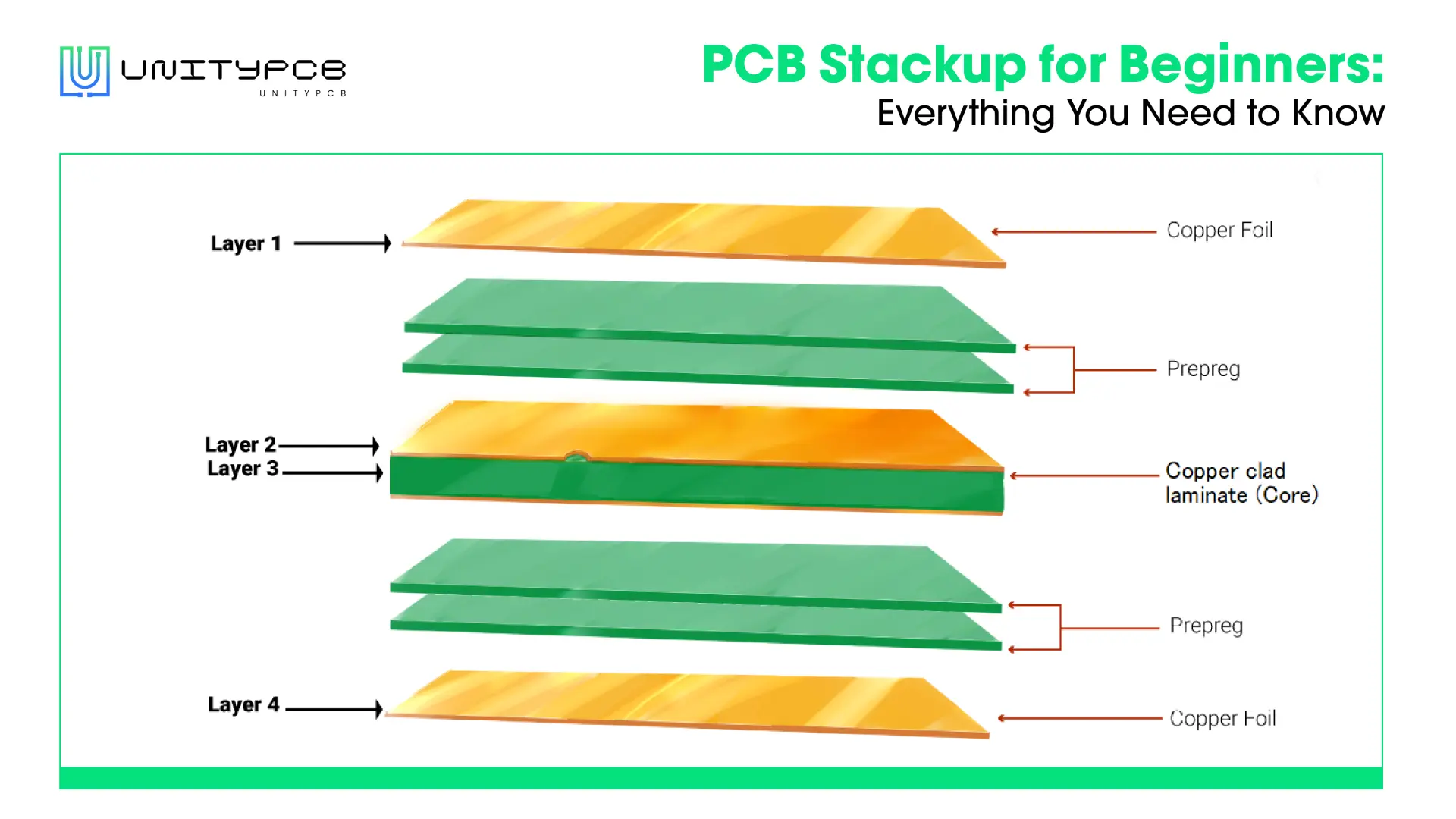
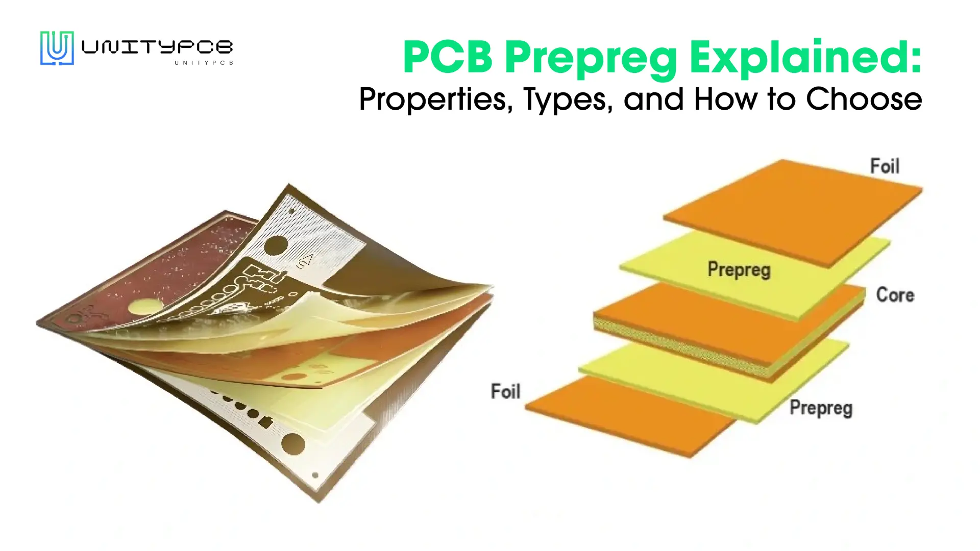
PCB silkscreen refers to a layer of ink printed on the surface of the circuit board to display component designators, part polarity, logos, symbols, and even test point locations.
Typically, PCB silkscreen materials are non-conductive epoxy inks that come in a variety of colors, such as white, black, yellow, and blue. However, white is the most commonly used color because it contrasts very well with the solder mask layer (regardless of its color), permitting easier viewing of the information. This layer is critical for assembly, troubleshooting, and component positioning on the PCB, as engineers and technicians can see visual cues to quickly identify components and test points.
Key Functions and Benefits of PCB Silkscreen
- Component Identification and Assembly
The silkscreen prints labels and designators (R1, C2, U1, etc.) directly on the PCB to show where each component belongs. These labels help assembly workers place components quickly and accurately. Without clear markings, workers might put components in wrong locations, leading to circuit failures and expensive fixes.
- Ease of Troubleshooting and Maintenance
Thanks to the silkscreen on the PCB, engineers and technicians can assess the component values (like resistor value or any type of capacitor) and parameters without the need of any external documentation. Repair PCB can be done with silkscreen easily as it allows you to know exactly where components are going to be located, helping reduce downtime, and reduce human error.
- Branding and Regulatory Information
Circuit board silkscreen can also serve a branding purpose. For example, manufacturers can print logos, trademarks and model identifiers, so their products can be easily identified. Moreover, safety certifications and compliance symbols (for example, CE, RoHS, UL) can be printed on the silkscreen to fulfil regulatory requirements.
- Aesthetic Considerations
The silkscreen can also add to the aesthetic appeal of a PCB. For example, when designing a PCB for consumer electronics, the neatly applied silkscreen can add a premium overall appearance to the finished product. It gives the product an appearance of professionalism which makes the product looks more ‘put together’ and lends weight to the manufacturer’s brand.
The Process of Applying PCB Silkscreen
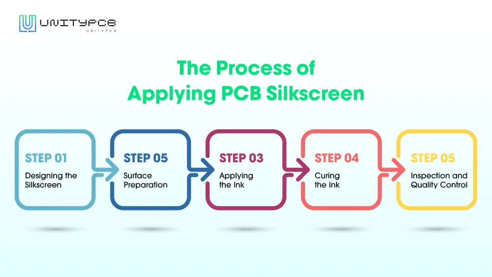
The process of applying the silkscreen layer involves several stages. Here’s an overview of the main steps involved:
- Designing the Silkscreen
During this phase, the PCB silkscreen layer is created using PCB design software such as AutoCAD or EAGLE. With these tools you can mark and label with symbols and text for identification and assembly. Once you’ve gotten to the final design, save the file in a format the PCB manufacturer can use.
- Surface Preparation
The surface of the PCB has to be very clean; any contaminant such as oil and dust must be removed before applying the silkscreen. Usually they are cleaned with a combination of ultrasonic and rinsing process.
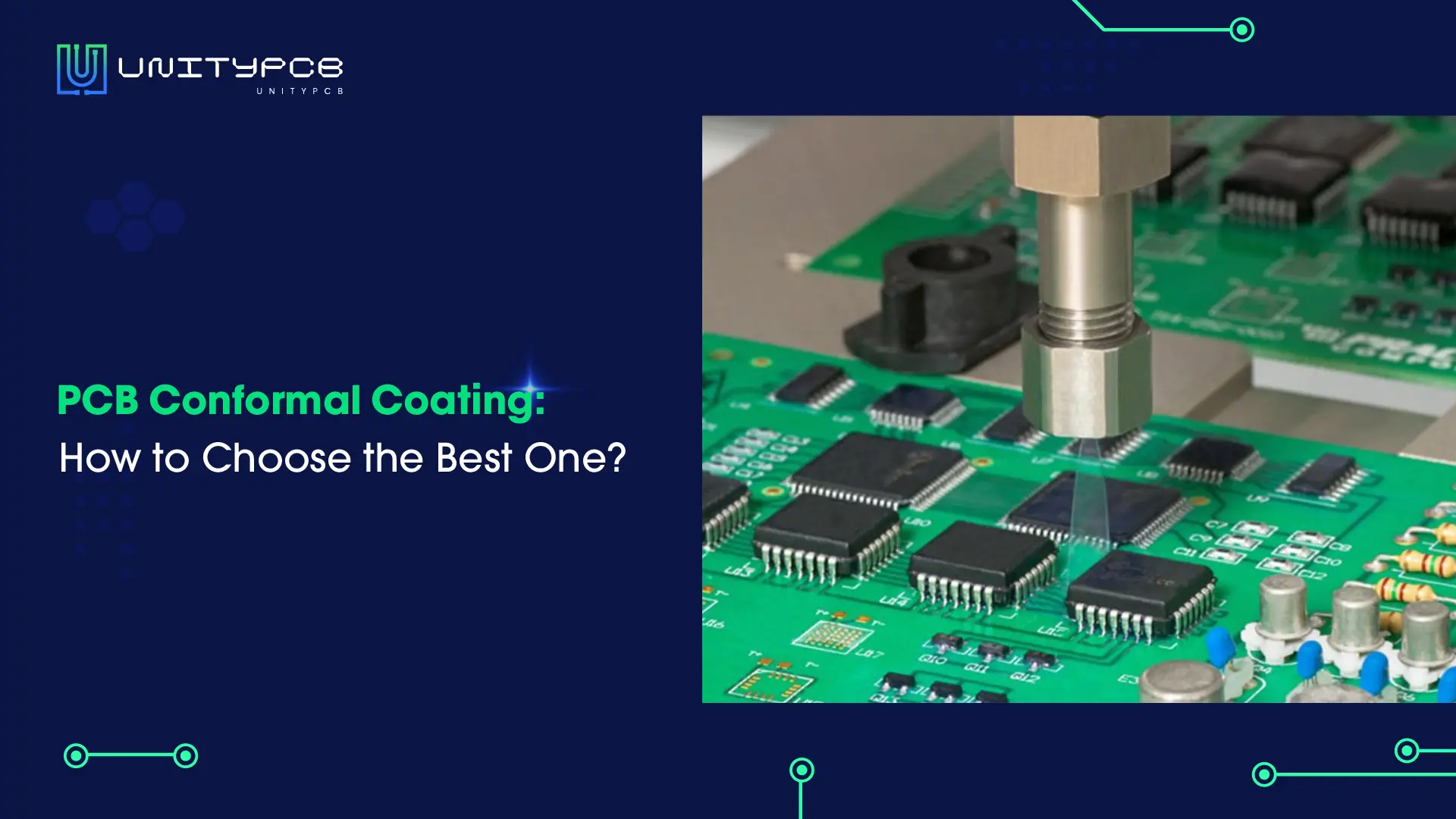
- Applying the Ink
Silkscreen ink is applied once the PCB surface is prepared. A stencil or mesh screen — usually stainless steel or polyester — is used to transfer the ink on to the PCB. Align the stencil with the PCB, then use a squeegee to apply the ink to the mesh openings and work its way through the openings, becoming printed onto the board.
- Curing the Ink
The ink then has to be cured after it is applied to make sure that it’s hard and will stick to the surface. Depending on the type of ink used, this step is usually done with a UV curing system or heat curing ovens.
- Inspection and Quality Control
After the silkscreen is applied and cured, the PCB receives a visual inspection and an automated optical inspection (AOI), ensuring clear, legible and properly aligned markings. This step is to catch any issues in the silkscreen application before the PCB moves onto the next stage.
3 Methods of PCB Silkscreen Printing
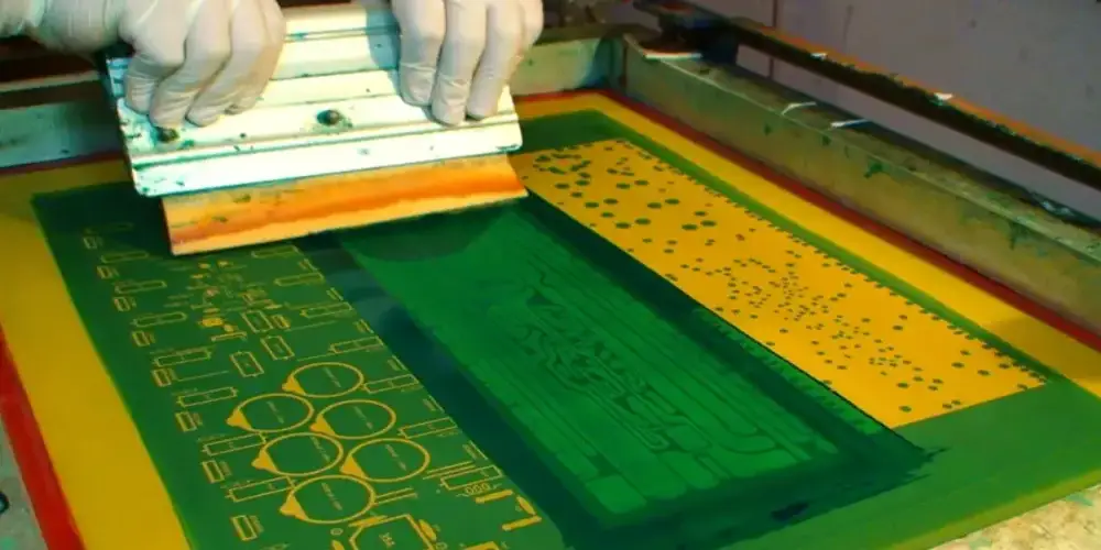
Manual screen printing
Manual screen printing is a conventional and economical way to print PCB silkscreen. In this method, epoxy ink is used. Technicians apply the ink manually on the laminate to obtain the impression when it is dried. Manual screen printing method has relatively simple setup requirements, which is often indeed attractive for many applications. Additionally, this method is most applicable to larger board sizes as the impression size is dominant; space must be available for the impression to effectively dry. When the target is just to cut down on expenses and board spacing is not a consideration, it is suggested that manual screen printing should be used.
Liquid photo imaging(LPI)
In liquid photo imaging, first, the laminate is coated with epoxy. It is then exposed to UV light so that image gets obtained. The results of liquid photo imaging are more precise than the manual silkscreening. Additionally, the board space required to implement this method is more efficiently used by reducing the spacing that is required. The downside is that this process takes more time for its setup along with application time,and may involve higher material costs compared to other methods.
Direct legend printing (DLP)
Direct legend printing (DLP) makes use of advanced inkjet printers that are capable of applying ink to circuit boards. It is a process where the PCB is directly printed on CAD application data. Acrylic ink is used for direct printing legend, and saving drying time. It is the most accurate and fastest method. It can accept a very low text height, but less than about 0.02 inches is not advised as the text will not be readable.
Design Considerations for PCB Silkscreen
- Font Size and Style: The front size and style must be readable and manufacturable. Typically, manufacturers work with text heights of 35 or 25 mil and a line thickness of 5 mil but other heights can be made with proper planning.
- Color Contrast: Choosing contrasting colors between the silkscreen and solder mask will make the silkscreen more visible. For instance, dark colors like black or blue with lighter backgrounds usually work well.
- Information Relevance: On the silkscreen layer, only include essential information. Avoid adding redundant information—this will clutter the design and confuse users.
- Spacing Requirements: Making sure that there is a adequate spacing between silkscreen elements and pads or vias to prevent overlapping, which can hinder soldering process.
- Manufacturer Guidelines: While there are general guidelines for design practice, you should still consult with your PCB manufacturer regarding their particular line width and spacing standards for silkscreen design.
- Testing Points: Clearly mark test points with appropriate identifiers so they can be easily located during testing phases without confusion.
Conclusion
Despite its understated appearance, the silkscreen layer is essential for ensuring that PCBs are functional and safe to use. From component identification to troubleshooting assistance and brand visibility, silkscreening is an indispensable step in the PCB manufacturing process. When manufacturers and designers really understand how to use silkscreen effectively, they end up with boards that work better, last longer, and look more professional.