
| Layer Counts | 6 layers |
| Base Material | Rogers |
| Bord Thickness | 1.6mm |
| Maximum PCB Size | 570*1200mm |
| Frequency Range | Up to 60 GHz |
| PCB Size Tolerance | ±0.2-0.3mm |
| Min.Hole Size | 0.1mm |
| Min.Line Width | 4mil |
| Copper Weight | 5oz |
| Surface Finish | ENIG, HASL, OSP are available |
| Certificate | UL , IPC-6012, RoHS, ISO 9001, ISO14001 |
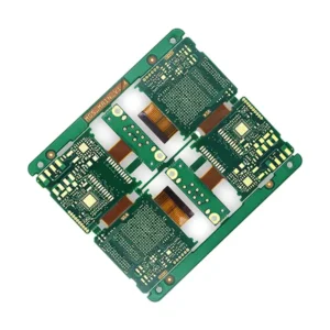
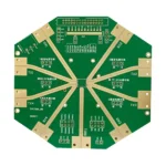 6 layer high frequency PCB
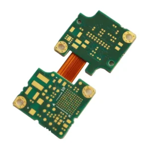
| 5 star | 0% | |
| 4 star | 0% | |
| 3 star | 0% | |
| 2 star | 0% | |
| 1 star | 0% |
Sorry, no reviews match your current selections