Elevate Your PCB Designs with Our Cutting-Edge PCB Via Technologies

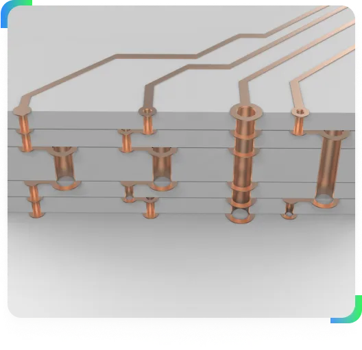
PCB vias play a crucial role in enabling high-density interconnections and facilitating efficient signal transmission. At UnityPCB, we use the state of the art via technologies and efficacy to create great performance. Our capabilities include through-hole, blind, buried, and microvia designs that enable product designers to work with complicated solutions and demanding specifications.
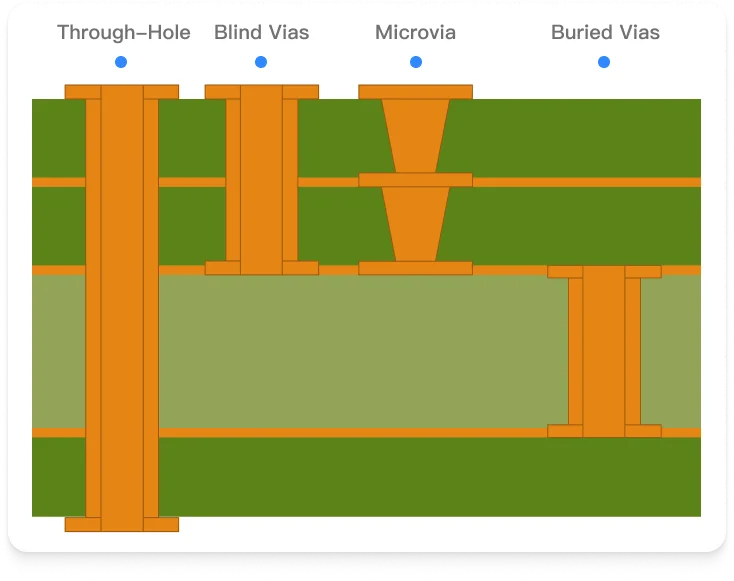
Through-hole vias traverse the entire board, adding extra mechanical stability and conductivity. They are sturdy and exhibit good mechanical strength as well as electrical connectivity, and are the best for components which need to be anchored strongly.
The blind vias connect the outer layer to an internal layer or more without passing through the whole board. For this reason, they enable more complex and denser tracks on multilayer PCBs.
Buried vias connect inner layers without reaching the outer surfaces of the PCB. These vias are non-exposed from the external side and allow for more complex layering and signal interconnection in multi-layer PCBs to further improve space and signal path usage.
Microvias are typically vias in HDI PCBs which are very small, having diameters lower than 0.15 mm. They are utilized to connect adjacent layers and can be stacked or staggered for even greater interconnect density.

| Drilling technologies | mechanical drilling, laser drilling, plasma drilling |
| Drilled hole size | 0.15mm - 6.30mm |
| Drill hole size tolerance | +0.13/-0.08mm |
| PCB through-hole diameter | 0.15mm-2.5mm |
| PCB through-hole diameter tolerance | 0.08-03mm |
| Min. copper thickness for via | 25um |
| Minimum via-to-via spacing | 0.2mm |
| Via fill types | Both conductive and non-conductive via filling |
| Advanced via technologies | Stacked vias, staggered vias, via-in-pad |
| Via backdrilling capabilities | Yes |
UnityPCB employs laser and precise mechanical drilling processes, leveraging advanced machinery to ensure high-accuracy vias with tight tolerances and consistent quality.
Our engineers can review your design and make suggestions to optimize and enhance the performance of your printed circuit boards.
We provide customized via solutions, so as to suit your specific requirements regarding the circuit design and performance.
At UnityPCB, we employ Automated Optical Inspection(AOI), X-ray inspection, and comprehensive electrical testing to ensure every via meets our stringent standards.
They are conducting through holes that allows signal and power to pass from one layer of this board to another. They are indispensable in providing design solutions for achieving dense interconnection in most of the modern electronics devices.
At UnityPCB we provide a number of different via options including through hole, blind, buried, as well as microvias.
Circuit board vias are usually made through drilling techniques including mechanical drilling techniques and laser drilling. The vias are then conducting plated with materials such as copper to provide the conductive barrels for the electrical connections.
UnityPCB’s engineers can recommend the most appropriate strategies for layout structures that would enhance the board functionality and signal quality.
The vias on the printed circuit boards can cause signal discontinuities and capacitive loading to pose problems to signal integrity particularly at higher frequencies. Therefore, an optimum via design is critical.
There are various aspects that should be considered while designing the PCB vias such as, aspect ratio of the vias, length of the via stub, clearance between the vias, clearance between vias and plane, etc.
Contact Us