When you pick up a printed circuit board, you’ll notice a network of tiny pathways on it. These are PCB traces, which enable electrical signals to be efficiently transmitted throughout the board. In this ultimate guide, we dive into PCB traces and discuss routing design considerations, routing design optimization tips, and how to repair traces. If you are just entering the field, this guide will give what you need to know about PCB traces.
What Is PCB Traces?

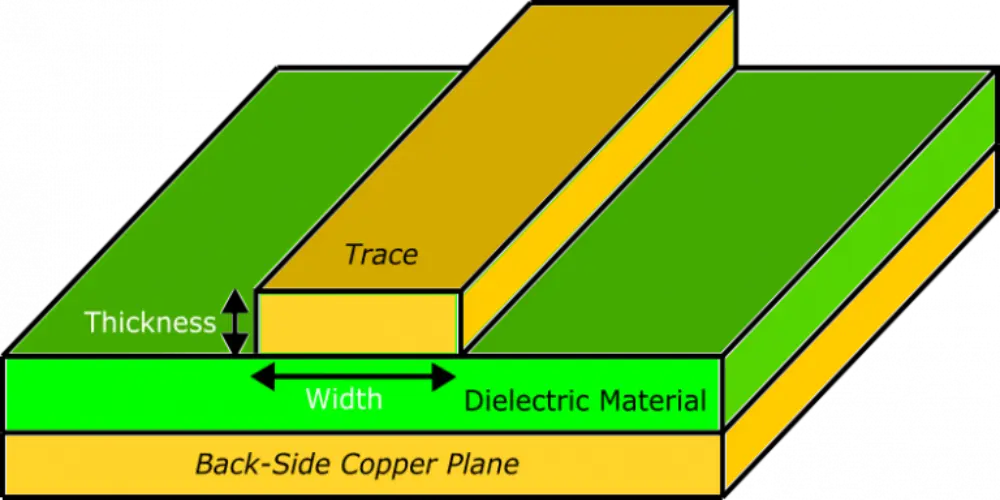
PCB traces are conductive pathways etched or printed on the substrate that can transmit electrical signals. These traces connect the components on the circuit board, allowing electrical signals to flow between the components for proper operation. They are carefully designed and laid out with specific width, thickness, and spacing to carry different currents and ensure the normal operation of the circuit board.
Materials of Circuit Board Traces
PCB traces transmit electrical signals, so the material used to make the traces must have high conductivity and stability. Copper has the advantages of excellent conductivity, easy processing, and low cost. Additionally, it has good thermal conductivity, which helps dissipate heat and keep the board within a safe operating temperature range. Therefore, copper is the most popular material for trace fabrication. It is not the sole option for material selection. Commonly used PCB routing materials include gold, silver, aluminum, etc.
Key Design Considerations for Effective PCB Traces
When designing PCB traces, factors such as PCB thickness, width, and spacing play a significant role in achieving optimal PCB performance and reliability. Let’s explore these key design considerations in detail.
1. Understanding PCB Trace Thickness

The thickness of traces on the board should be as uniform as possible. Uneven thickness can cause impedance mismatch, signal reflections, and crosstalk, which can affect circuit performance. The PCB trace thickness also needs to be adjusted according to the structure and type of the circuit board.
PCB copper trace thickness is measured in ounces. Ounces is a measure of weight rather than thickness. One ounce of copper, when evenly distributed over a 1 square foot area, results in a 1.37 mil thick copper layer. Using a uniform standard (1 oz/sq ft), PCBs from different manufacturers can maintain consistent physical and electrical characteristics. Generally, manufacturers default to a standard trace thickness of 1 ounce for PCBs unless otherwise specified in the design documentation. For PCB designs with high voltage or special resistance or impedance requirements, a thicker copper layer may be required.
2. Calculating PCB Trace Width
PCB trace width directly affects current carrying capacity, signal integrity, and thermal management capabilities. It is usually measured in mils. The standard trace width for common signals ranges from 7 to 12 mils. Too much current through a trace can cause the temperature to rise, affecting the performance of the board or even damaging it. Wider traces have lower resistance and can carry higher currents without overheating. Choosing trace width depends on many factors, including the current carried, operating temperature, available routing space, manufacturing constraints, etc.
3. Setting Trace Spacing

The distance between two neighboring traces is referred to as PCB trace spacing. This parameter is crucial to prevent crosstalk and electromagnetic interference. Appropriate spacing can reduce electromagnetic field coupling between traces and avoid affecting signal integrity. Especially in high-frequency circuits, specific spacing may be required to reduce crosstalk, reflections, and coupling. Interference with the signal may cause data corruption. Designers can more effectively control trace spacing and ensure circuit stability and reliability with the guidance of standards such as IPC-2221 and IPC-2141.
How to Calculate Trace Width?
In the PCB industry, there are many calculators that we can use that follow industry standards to calculate trace width. IPC 2152 and IPC 2221 are two of the most common standards, which we will cover in depth below.
IPC 2221:
IPC 2221 is derived from the older standard IPC-D-275 that was used. It not only provides methods for trace width calculations but also contains more extensive PCB design guidelines. The IPC 2221 calculator uses a chart and formula to help designers determine the current carrying capacity of traces in the circuit board. The calculator uses the equation “I=kΔTbAc” to calculate the trace width.
The variables in the formula are represented as follows:
- I: Electric current, its unit is ampere.
- K: Constant, depends on the position of the trace. For visible traces, K is 0.0048. For internal traces, k is 0.024.
- ΔT: Changes in temperature are measured in Celsius.
- A: The trace’s cross-sectional area.
- b: The value is 0.44.
- c: The value is 0.725.
Using this formula, a specific range of values needs to be considered when calculating the trace width. This ensures the accuracy of the calculation.
- Current Range: Between 0 and 35 amps.
- Trace Width: Between 0 and 10.16 mm.
- Copper Thickness: Between 0.5 and 3 oz.
- Temperature Rise: Between 10℃ and 100℃.
IPC 2152:
IPC-2152 is a more modern standard specifically for calculating PCB trace widths. Compared with the traditional IPC-2221, IPC-2152 adopts more advanced technical methods. Thus, it provides a more accurate maximum trace current calculation. When using this calculator, we must rely on computer-integrated general charts to obtain the unadjusted cross-sectional areas. The calculator takes into account various parameters to compute the right trace width.
Useful Tips for Optimizing PCB Traces Routing
Smart Use of PCB Auto-Routing Tools
PCB design software can perform automatic routing, which saves time and is an effective way to route. Automatic routing cannot be used as the only complete solution. It may miss critical or special design requirements. Combining automatic routing and manual routing is the most effective method. Use automatic routing for initial basic routing, and then manually optimize the PCB layout to obtain the best path based on the design requirements.
Selecting the Correct PCB Trace Width
The trace width must match the trace capacitance to have a smooth current flow. The minimum width of a trace must be accurately determined. If not done so, it might overheat the board and impact thermal management. Proper trace width will also reduce the risk of disconnection.
Designing Effective Ground Planes
The ground plane provides a consistent reference for voltage measurements on all traces. It is important to design a continuous ground plane, across the entire copper area or by using a full-layer ground in a multilayer board. Placing a ground plane underneath signal-carrying traces can reduce impedance and increase noise immunity.
Avoiding Capacitive Coupling
To reduce capacitive coupling caused by routing above and below a large ground plane, power, and analog signal lines should be routed separately on dedicated layers to avoid coupling. Decoupling capacitors are an effective and economical solution.
How to Repair PCB Traces?: A Step-by-Step Maintenance Guide
When the power supply unit displays faults or makes unusual noises, it means that the PCB traces need repair. After understanding the relevant knowledge of tracing, it is also important to know how to repair it. Let us explain it step by step.
Step 1: Find damaged traces on the PCB, such as breaks, corrosion, etc. A microscope or magnifying glass can be used to detect minute flaws that are not visible to the human eye.
Step 2: With the use of a cutting tool, cut away and remove the damaged trace. Do not damage surrounding traces, contacts, or components. Clean the repair area of coating particles and other residues.
Step 3: Apply flux to the trace and tin each end of the trace using a soldering iron and solder wick.
Step 4: Select a new wire to replace the old one.
Step 5: The insulation is removed from the ends of the wires and tinned with solder.
Step 6: Overlap the new wire over the existing trace and apply flux to the overlap, soldering them together. The overlap distance is at least twice the trace width.
Step 7: Use the wire tool to create the required wires to match the PCB design.
Step 8: Attach the wires to the board, using tools such as adhesives and tape dots to keep the wires firmly attached to the board.
Step 9: Solder the other end of the wire as well. The repair is nearly finished. Make sure the connection is functioning correctly. At the same time, clean up the remaining stains.
Final Words
Appropriate PCB traces are critical to the function and reliability of electronic devices. From determining PCB trace thickness, width, and spacing to overall routing, each factor plays an important role in achieving optimal product performance. PCB trace design becomes more challenging as PCBs get smaller and more intricate. Mastering the basic PCB trace knowledge will help you do a good job on PCB routing.


