PCB stackup design is the key to manufacturing multilayer circuit boards. Reasonable stacking can optimize PCB electrical performance and reduce manufacturing difficulty. Regardless of whether you are a novice or an engineer, this article will provide you with all that you want.
What Is PCB Stackup? Why Is It Important?
PCB stackup is the arrangement of layers in a circuit board, including conductive copper layers (for signal, power, or ground) and insulating dielectric layers. It defines the PCB structure, affecting its mechanical stability, signal integrity, and electrical performance. Then, let’s explore why PCB stack-up is important.
Determine PCB Electrical Performance: A good PCB stackup design optimizes power and signal distribution. By properly laying out the power, ground, and signal layers, parasitic capacitance and inductance can be minimized which can degrade PCB performance. This optimization can improve signal transmission speed and power delivery to each part of the circuit.
Improve Signal Integrity and Reduce Noise: By increasing the spacing between traces or isolating the analog and digital parts of the circuit, crosstalk and electromagnetic interference can be effectively reduced. Besides, selecting insulating materials with low dielectric constants can guarantee cleaner signal transmission and further reduce noise.
Affect Electromagnetic Compatibility (EMC) and Reduce Emissions: A well-designed PCB stack-up effectively addresses EMC issues by integrating adequate shielding, achieving proper impedance matching, and optimizing trace spacing. This can effectively minimize electromagnetic radiation and electromagnetic susceptibility, allowing the PCB to not interfere with external electronic devices while also being unaffected by them.
Different Types of PCB Stackups
Thanks to advances in laser drilling, sequential lamination, flexible substrates, and more, we are able to create more compact and advanced PCBs. Below are several types of PCB stackups to suit different application requirements.
Standard Multilayer PCB Stack-Up
These stackups typically consist of three or more copper layers insulated by a core layer or prepreg and interconnected using PCB vias. Since they are manufactured in a single lamination cycle, the circuit board is subject to less thermal stress and mechanical pressure. This standard multilayer PCB stackup doesn’t require laser drilling, which reduces processing difficulty, saves production costs, and shortens manufacturing cycles. Here are some common PCB stackups and their features:
- 4-layer PCB stackup: The 4 layer board stackup includes 4 layers: top, bottom, and two inner layers. The top and bottom layers are employed for signal routing, while the inner layers are typically devoted to power and ground planes to enhance signal integrity and reduce EMI.
- 6-layer PCB stackup: It consists of 4 signal layers and 2 inner layers for power and ground. This stack-up allows for efficient signal routing and better return paths, which is critical for high-speed applications.
- 8-layer PCB stackup: The 8 layer stackup includes four signal layers, two power layers, and two ground layers that are carefully arranged to optimize signal integrity and reduce electromagnetic interference. Strategic placement of the power and ground layers in the center provides excellent capacitance and thermal management, while the additional layers enhance routing flexibility.
For more complex and high-performance designs, advanced PCB stack-ups such as 10 layer PCB stackup, 12 layer PCB stackup, etc, could be employed.
Metal Core PCB (MCPCB) Stack-Up
They are commonly used in high-power LEDs and other high-power delivery applications. The metal core (typically aluminum) affects the overall PCB thickness and also performs two key functions: heat dissipation and electrical conductivity. Firstly, it effectively disperses the heat generated by ICs and other PCB components during operation. Secondly, the core ensures the flatness and conductivity of the bottom layer of the circuit board, allowing it to be stably connected to the external heat sink.
HDI PCB Stack-Up
HDI PCBs include blind vias, buried vias, and microvias to support ultra-compact digital circuit designs. These designs often feature a high-performance processor with very fast data buses, including connections with memory and external serial and parallel peripherals (PCI-connected devices). HDI PCB uses very small non-standard vias, precisely controlled impedance traces, and HD footprints with tight clearance and solder mask requirements to accommodate a variety of layer configurations.
High Frequency PCB Stack-Up
High-frequency PCBs are made to handle high-frequency signals (up to 100 GHz) and are often utilized in RF-intensive applications. These PCBs have some special design requirements, such as precise tolerances for clearance and spacing, trace antenna design, and strict control of solder amount used on connectors, all of which ensure that the circuit can operate efficiently and stably under high-frequency conditions.
Flex and Rigid Flex PCB Stack-Up
These PCB stackups are specifically designed for compact and adaptable applications such as portable and wearable devices. These boards can be fully flexible or a combination of flexible and rigid to create a single circuit board assembly that can adapt to different shapes and movements. Flex boards are composed of a flexible polymer substrate, copper layers (one or more), and an overlay. They can connect circuits through traces and vias like a standard PCB while having the ability to bend.
PCB Stack-Up Design Considerations
When designing a PCB stackup, it is essential to consider below key factors to create a reliable and manufacturable design.
PCB Lamination Methods
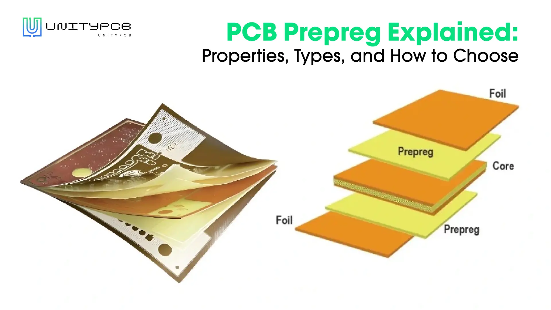
PCB lamination is the process of laminating inner layers, prepreg and copper foil by heat and pressure to form a multilayer circuit board. There are two common methods to laminate PCB: foil construction and cap construction.
Foil Construction
Foil construction is widely used in PCB lamination because it can accurately ensure the accuracy of layer-to-layer alignment and drilling positions, making it easier to manufacture. Besides, this process requires less core substrate material, reducing manufacturing costs.
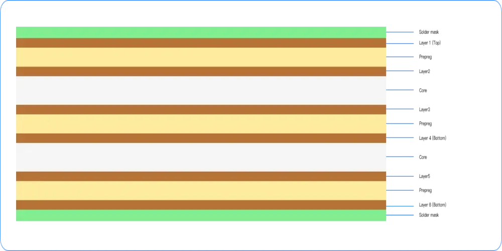
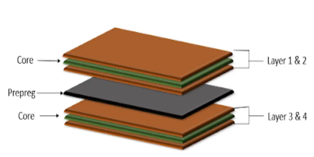
In foil construction, prepreg is located between the outer copper foil and the inner layers. For instance, prepreg is situated between the first and second layers as well as between the third and fourth layers of a four-layer PCB. The outermost copper layer is not made of copper clad laminate like cap construction but is a continuous sheet of copper foil. This is a 4 layer PCB stack-up for better understanding:
- Top Layer (layer 1)
- Prepreg
- Inner Layer: Laminate PCB core (layer 2 and layer 3)
- Prepreg
- Bottom Layer (layer 4)
Cap Construction
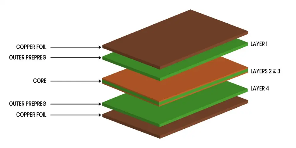
In cap construction, the two outer layers are built with pre-copper clad laminate and separated by a single prepreg layer (take four layer PCB as an example). This is a PCB stackup showing the cap construction of a 4 layer PCB:
- Layer 1 and layer 2: Soldermask applied to the outer laminate layer
- Prepreg
- Layer 3 and layer 4: Soldermask applied to the outer laminate layer
This method is not recommended in modern PCB manufacturing, except for hybrid PCBs where special laminates need to be manufactured and certain drilling methods (such as laser drilling) are not available.
Types of PCB and Their Applications
For PCBs that contain a large number of power components or need to carry high current traces, it may require adding multiple layers to place power planes or copper-filled areas to reduce resistance and heat dissipation. Radio frequency components (such as RF switches or modems) require multiple planes to help dissipate heat and provide better grounding. Circuit boards with sensitive digital domains (such as Ethernet, PCI, etc.) are usually designed with dedicated internal layers to add additional ground planes.
PCB Component Density
PCB component density affects the stacking design, especially when using high pin count processors or BGA packages. Due to smaller pitches and complex pin patterns, it may require additional layers to achieve reasonable signal routing.
Component Types and Interfaces
The choice of component type and interface (such as digital, mixed signal, analog, or high-speed signal) will affect the PCB stack-up design. Although using BGA (ball grid array) components can save space, it increases production costs and manufacturing complexity, and rework is difficult.
Mechanical Requirements
Mechanical stability is critical in PCB stack-up design. Thinner boards save space but risk warping and vibration, while thicker boards provide enhanced durability and support for components. The number of layers and dielectric spacing must match the mechanical requirements of the design to ensure structural stability and end-product reliability.
5 Tips for Designing an Efficient PCB Stackup
Though PCB stack-up design depends on different application requirements, here are some general guidelines that can help create a better design.
- Choose the right dielectric material to meet the mechanical, electrical, and thermal properties required by the PCB design. For high-frequency circuit boards, choose low Dk materials. The thickness of the copper plane is closely related to the amount of the current. For circuit boards with high current, the copper plane needs to be thicker.
- Estimate the number of signal layers required based on different application requirements. High-power or high-speed applications will require more signal layers than low-speed one
- Reasonable planning of the number of power layers and ground layers can greatly improve the signal integrity and EMC performance of the PCB.
- Carefully design the trace width, spacing, and layer stackup to ensure uniform impedance across the high-speed trace for good signal integrity. To avoid signal distortion, ensure a stable ground plane underneath the controlled impedance trace and account for the trapezoidal effect of the trace when calculating impedance.
- The arrangement of sequential layers is an important aspect to consider in PCB stack-up. Signal layers, ground layers, and power layers need to be placed alternately to reduce EMI. These are useful tips for arranging the layers.
- Keep the stack-up symmetric. Even-number-layer PCBs have cost advantages and are more resistant to board warping than odd-number-layer PCBs.
- Do not put two adjacent signal layers since this might easily cause crosstalk.
- The signal layer is usually arranged on an adjacent layer to the ground layer or power layer to provide a low-impedance signal return path.
- The power plane and ground plane should be as close as possible.
- Use complete power layers and avoid unnecessary splitting. Keep two adjacent power layers as far away as feasible to avoid unnecessary coupling.
Final Words
Designing an efficient PCB stackup is a critical step to ensure board performance, reliability, and manufacturability. Proper stackup design is essential for achieving PCB optimal signal integrity, thermal management, and power distribution. As a new or experienced engineer, comprehensive knowledge of the PCB board stackup will help optimize design and streamline production.