PCB pads play a critical role in the PCB assembly process, serving as the foundation for soldering the components. The soldering quality will be impacted by the PCB pads’ size, shape, and spacing. Well-designed printed circuit board pads are essential to ensure reliable electrical connections, rugged mechanical stability, and long-term performance of assembled components. You will learn everything you want to know about PCB pads in this blog, from what are they to key design considerations.
What Are PCB Pads?
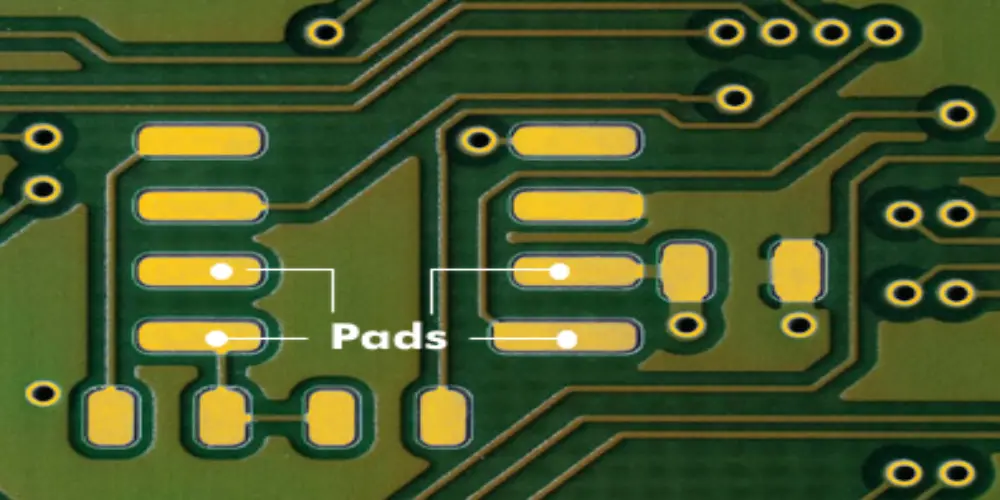
PCB pads are exposed metal areas on a printed circuit board (PCB) used to solder component pins or leads. When multiple pads are arranged in a specific pattern on the PCB, they form a component footprint or land pattern that matches the physical and electrical requirements of the components.
What Are Pads Made Of?
The PCB pad material has a direct impact on the board’s solderability, electrical performance, and durability. The most popular material for pads is copper due to its superior solderability and conductivity. However, it tends to oxidize in exposed environments. The PCB pads need to process a PCB surface finish (HASL, ENIG, or OSP) to improve solderability and prevent oxidation.
Types of PCB Pads
Now that you understand the basics of PCB pads, let’s look at the essential types of PCB solder pads.
Surface Mount Pads
Components can be soldered directly into pads on the PCB surface without drilling. Surface mount pads are ideal for small components (resistors and capacitors), as well as integrated circuits (QFP and BGA chips) installation. These SMT components can be assembled to the board using surface mount technology, which can highly increase production efficiency.
Key Features:
Precise Pad Design: The pad design of the printed circuit board matches exactly with component pins to create a dependable connection.
Compact Design: These PCB pads support a high-density component layout. They are particularly advantageous in multi-layer circuit boards and can support complex and compact circuit designs.
Automated Production: The pad design is suitable for the SMT automatic production process. The soldering can be quickly completed through automatic machines, including the component placement machine and reflow oven. This is conducive to improving production efficiency and is suitable for large-scale production.
Ball Grid Array (BGA) Pads
The pads are a special type of surface mount pads that are specifically used for BGA components. BGA pads come into two types: solder mask defined and non-solder mask defined.
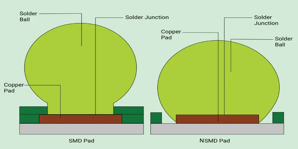
1. Solder Mask Defined (SMD) BGA Pads
The shape and size of the SMD pads are defined by the apertures in the solder mask. The solder mask surrounds the edge of the PCB pad, creating a slight overlap between the pad and the solder mask, which minimizes the exposed area of the copper layer.
Here are the advantages:
- The solder mask overlaps the periphery of the pad to provide additional support.This can prevent the pad from shifting or falling off.
- The soldermask precisely controls the pad size to ensure even solder distribution and minimize false soldering or bridging.
- This helps to accurately align the BGA solder balls to improve soldering quality.
- The solder mask reduces the exposed area ofthe pads. The risk of solder bridging or short circuits can significantly be decreased, making it suitable for high-density designs.
2. Non-Solder Mask Defined (SMD) BGA Pads
An NSMD pad’s size is determined by the pad diameter, not the solder mask opening. There is a small gap between the solder mask and the pad, leaving the pads fully exposed.
Here are the advantages:
- It is widely used for high-density and fine-pitch BGA chips.
- This is easy to solder and more stable solder joint quality.
While NSMD pads have a major drawback. This type of PCB pad is sensitive to thermal and mechanical stresses. It is easy to cause delamination problems. The risk can be highly decreased through strict adherence to standard manufacturing and handling processes.
Through-Hole Pads
Through-hole pads are mainly used to install through-hole components. It requires drilling holes in the PCB, and passing the component pins or leads through the holes. They are then soldered on the pads. There are two main categories: PTH pads and NPTH pads.
1. Plated Through Hole (PTH) Pads
The hole of the PTH pad needs to be electroplated to form a conductive metal layer. This electroplating ensures the electrical connection between the PCB pads and the PCB layers.
2. Non-Plated Through Hole (NPTH) Pads
After drilling, the hole of the NPTH pad is not plated. This pad is only used for mechanical fixing or heat dissipation and cannot achieve an electrical connection.
Key Features:
High Mechanical Strength: The component pins are inserted into the PCB holes and soldered to the pads, providing mechanical and electrical dual connections. This is suitable for application scenarios with high mechanical stress.
Large Size and High-power Components: Through-hole pads are often used for soldering larger components (such as connectors) and high-power components. This PCB pad can be connected to the internal copper layer and can withstand greater current and heat loads.
Manual Soldering and Easy Repair: This pad has a simple design and the component soldering process is direct and simple. Components can be manually soldered to through-hole pads, which also provides convenience for later repairs and replacements.
Other Functional Pads
Here we also introduce two types of PCB pads with specific functions.
1. Thermal Pads
Thermal pads are designed for PCB thermal management. This type of pad is often used for components that need to dissipate heat to ensure that they can operate at a safe temperature. These pads can transfer the heat generated by the components to the copper layer or heat sink.
2. Test Pads
Test pads are tiny exposed copper areas on the circuit board surface. This is the point used to test and debug the PCB. These pads facilitate circuit board electrical testing (voltage, current) to verify their function.
Why PCB Pad Size, Shape, and Spacing Matter
When designing the PCB pad, the right size, shape, and spacing of the pads are key factors in determining soldering quality and circuit reliability.
PCB Pad Size and Shape
The size and shape of the PCB pad directly affect the quality of component soldering. A pad that is too large can cause solder bridging, and a pad that is too small will result in weak solder junctions. Single-sided pads usually have a 1.6mm width, which is suitable for most through-hole components. If the component needs to soldering on the PTH pads, the PCB pad diameter needs to be increased by 0.5mm. This can improve mechanical strength and adapt to larger vibrations and shocks.
Special pad shapes become necessary for pads that exceed 1.2mm aperture and 3.0mm diameter. It can be designed with oval or teardrop shapes, which can optimize space utilization. Teardrop-shaped pads help to disperse mechanical stress and reduce the risk of solder joint cracking.
PCB Pad Spacing
PCB pad spacing must match the dimensions of component pins during the design phase. If the axial component pin diameter is less than 0.8mm, the pad hole spacing is usually 4mm larger than the standard spacing of the component itself. If the axial component pin diameter is greater than 0.8mm, it needs to be 6mm larger. This is because the solder and component pins will expand due to heat changes during the soldering process. Increasing the spacing can effectively reduce mechanical stress concentration.
Key Considerations When Designing PCB Pads
When designing pads, there are many factors that need to be considered to ensure the reliability and manufacturability of the circuit board.
Termination Style
Different components, such as capacitors, resistors, ICs, connectors, etc., all have different termination styles. Surface mount chips require rectangular pads. Whereas axial lead resistors need round pads with holes. The geometry of the pads needs to match the component termination style to ensure good soldering quality.
Reliable Connections
Heavy or large components like connectors need extra support to maintain operational stability under vibration conditions. For reinforcement, you can use extra anchor pads or large pads.
Signal Integrity
The design of PCB pads requires attention to both signal integrity and electrical performance of circuit boards. The PCB solder pads are well-integrated with impedance-matching traces. The crosstalk is reduced through a reasonable PCB layout. After the design is completed, it’s essential to use design software to perform simulation verification and validate through prototype testing.
Production-Friendly Design
Pad design requires a proper balance between manufacturability and cost. The limitations of drilling and plating processes also need to be considered. When designing pads, it is necessary to strictly follow the design for manufacturing (DFM) principles and comply with industry standards.
Last Words
Properly designed PCB pads are a critical factor in ensuring successful PCB assembly and long-term component reliability. This is what UnityPCB can help you. If you have any questions about PCB pad design, contact us for professional advice. With nearly 20 years of rich manufacturing experience, we commit to providing one-stop PCB & PCBA services, including PCB design, component sourcing, PAB manufacturing, PCB assembly, quality control, etc. UnityPCB adheres to a strict quality management system and has obtained ISO, IPC, RoHS, and other certifications to ensure that each of our PCBs and PCBAs meets high-quality standards.