At UnityPCB, we have state-of-the-art facilities, along with a team of skilled personnel who put in the best effort to deliver printed circuit boards with superior quality, meeting even the most stringent requirements. Our comprehensive manufacturing capability covers many types of materials, technologies, and product types, and as a result, we are able to serve a very wide spectrum of our clients from different industries. Explore our PCB capabilities below to see how we can support your next project.
| Features | Capabilities | Patterns |
|---|---|---|
| PCB Layers | up to 18 layers | / |
| Substrate Materials | FR-3, FR-4, FR-5,CEM-1, CEM-3, RCC,metal, ceramic, thermoplastic | / |
| Min. PCB Size | 10*10mm | 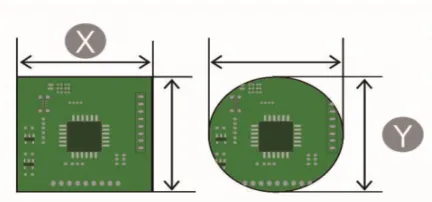 |
| Max. PCB Size | double-sided: 570*1200mm Four-layer: 570*850mm, Six layers and above: 570*670mm | |
| PCB Size Tolerance | ±0.2-0.3mm(depends on the size of PCB) | / |
| PCB Thickness | standard:0.8mm-2.0mm Non-standard: 0.3mm-5.0mm | 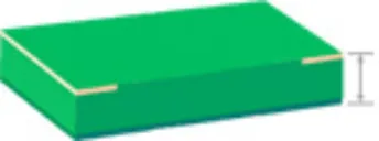 |
| PCB Thickness Tolerance | ± 0.1-0.25 mm PCB board thickness ≥3mmthe tolerance is ±10% | / |
| Min. BGA Pad Size | 7mil | 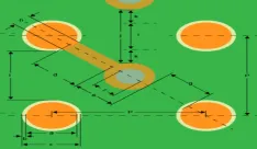 |
| Outer Layer Copper Thickness | 0.5-5 OZ |  |
| Inner Layer Copper Thickness | 0.5-2 OZ |  |
| Min. Line Width | 4mil | 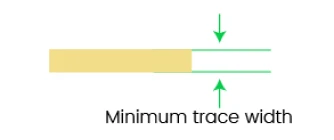 |
| Min. Outer Layer Line Spacing | 4mil - 7mil | 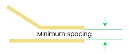 |
| Min.Inner Layer Line Spacing | 4mil - 7mil | |
| PCB Through Hole Diameter | Standard: 0.3mm-2.5mm Extreme: 0.15mm | 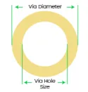 |
| Min. Drill Slot Tolerance | Slot width direction: ±0.1mm, Slot length direction: ±0.15mm | 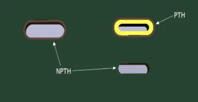 |
| Min. Milling Slot Tolerance | Slot width and length direction: ±0.15mm | |
| Min. Via Copper Thickness (through hole) | 25um | 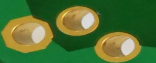 |
| Min. Via Copper Thickness (buried/blind holes) | 20um | 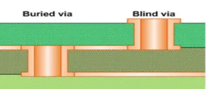 |
| Rigid-Flex Peel Strength | ≥1.4N | / |
| Pad Surface Treatment | HASL, ENIG, OSP, ENEPIG, I-Ag, I-Sn | / |
| Gold Finger Gold Plating Thickness | 0.25-1.3um | 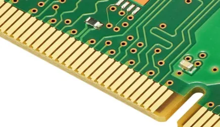 |
| Gold Finger Nickel Plating Thickness | 3-5um | |
| Solder Mask Color | Green ,Red, Yellow, Blue, White ,Black, Purple | 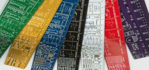 |
| Min. Solder Mask Thickness | 10um |  |
Contact Us