Tailored PCB Layer Stackup Solutions for High-Performance Designs
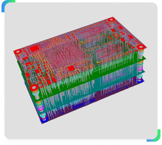
The PCB layer stackup refers to the arrangement and sequence of copper and insulating layers in a multilayer PCB. UnityPCB creates highly detailed and advanced layer stackup configurations to meet different needs of our clients. The stackups we design and implement have been uniquely optimized for high speed and density circuits, as well as for improving performance in accordance with different application needs under various standards of the industry.
A 4-layer PCB stackup is created with two layers of signals and two internal planes for power and ground. This configuration improves signal signal integrity and signals EMC or electro magnetic compatibility, which makes it appropriate for moderately circuit complexity.

The Six-Layer PCB layout consists of four signal planes and two internal planes for power and grounds. This arrangement comes with enhanced signal quality, lower inter-channel interference, and adequate power supply, allowing it to be ideal where complex circuitry is required.
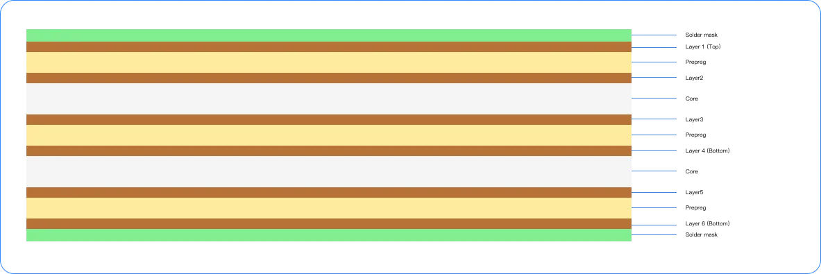
It comprises of six signal layers and two internal power/ground planes. This design configuration provides superior signal integrity and EMI performance, suitable for high speed signal and intricate routing, and for systems that require high data processing rates.
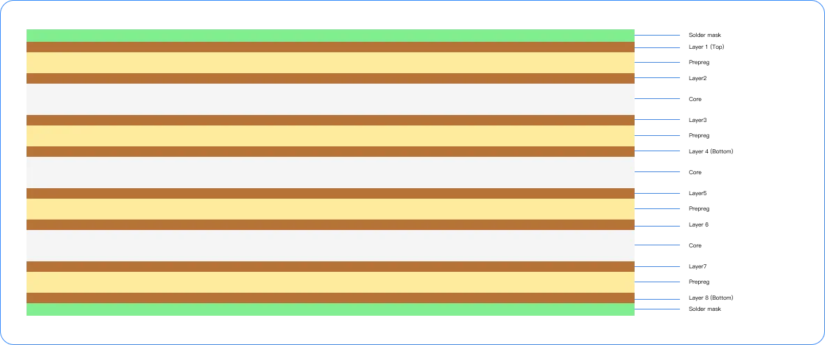
A stack up of 10 layers is designed with eight signal and two plane layers respectively. This structure offers better signal quality, signal interference or crosstalk, and power transmission, which fulfills requirements of high integration density and high performance computing, communication and industrial automation applications.
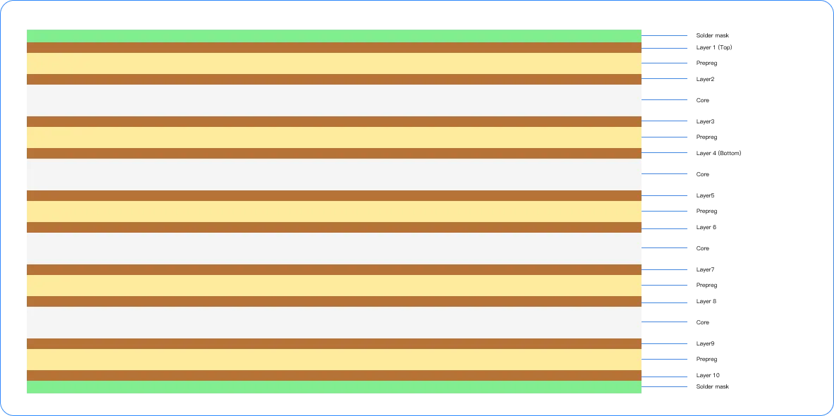
This PCB board stackup has ten signal layers and two internal planes for the power and ground. It also has highly advanced speed and frequency to enhance performance, minimize interferences, and provide efficient power supply management.
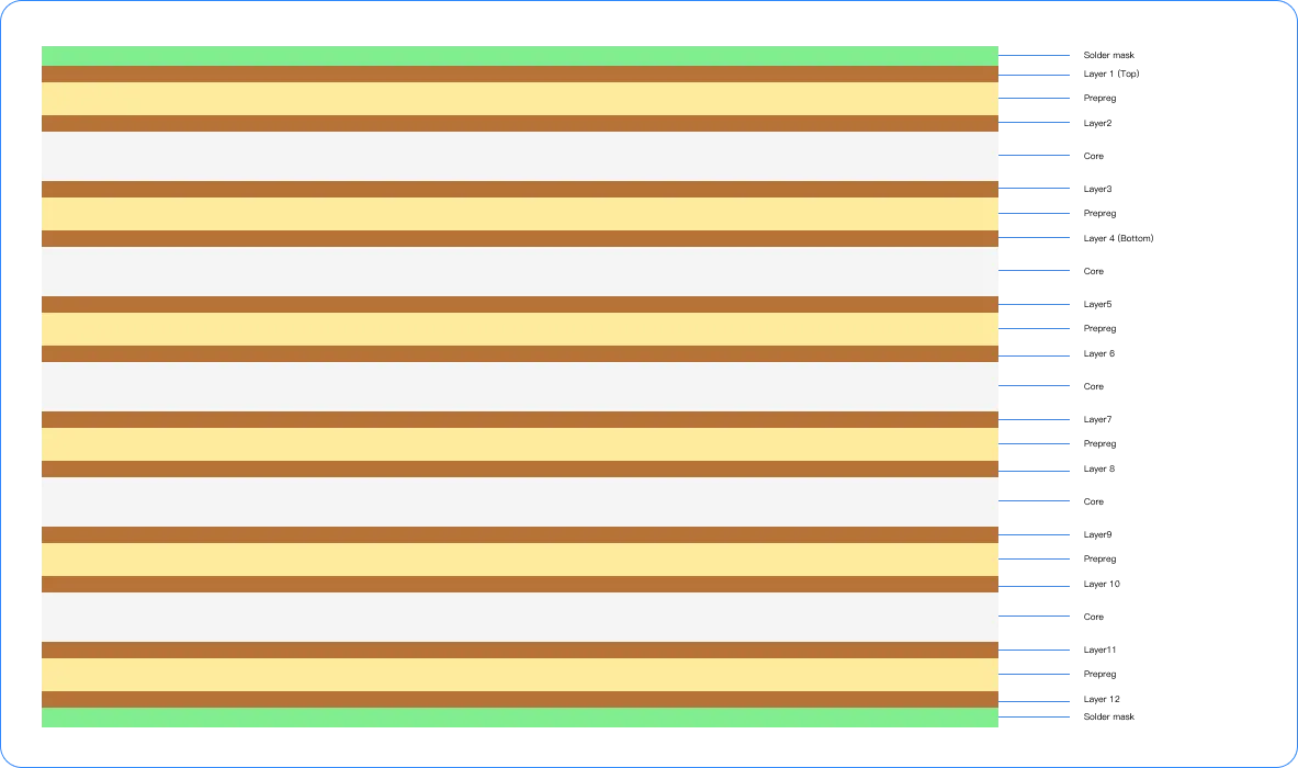
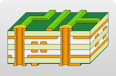
Customized layouts and consultation regarding the choice of materials, electromagnetic interference, and heat dissipation for the highest efficiency and endurance.
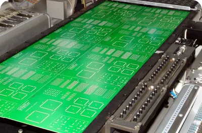
Fast prototyping alongside efficient production processes in order to achieve the designed performance, quality, and delivery to meet schedule.

Our engineers are available to provide help and advice at the design , manufacturing and after production stages.
Our engineers have nearly 20 years of experience in designing the PCB layer stackup, providing reliable solutions for customers in various industries.
Effective DRC checking as well as DFM optimization assures compliance with industry standards, , fabrication limitations and achievable fabrication cost.
We offer customized stack-up solutions that match specific design requirements. Whether it’s a simple two-layer circuit board or a much more complicated multi-layer design.
Support and documentation are offered throughout the project and individual steps to provide the best PCB layer stackup solution.
A PCB stackup refers to the arrangement of copper and insulating layers in a printed circuit board, which is crucial for its functionality and performance.
PCB stackup is an important design parameter that can affect signal integrity, thermal management, and electromagnetic compatibility of the PCB and hence can affect the reliability of electronic devices.
Some crucial factors that need to be considered when designing the stackup of PCB include the layers of the material, the impedances, thermal management, and signal integrity.
Yes, UnityPCB offers custom stackup design services tailored to your specific project requirements.
PCB stackup influences the speed of signal transmission through controlling the impedance and avoiding signal distortion, while reduction of EMI through the correct approach to grounding and shielding.
We implement the best practices of PCB stackup designs, carry out tests every step of the process and implement strict quality standards to ensure the functionality of UnityPCB.
Contact Us