PCB drilling is the process of creating precise holes in a bare PCB to mount components or connect different layers. The drilling process must be performed precisely and accurately, as even the smallest error can have a disastrous effect on the PCB quality. By understanding PCB drilling, manufacturers and designers can make their PCBs more dependable. This is a complete introduction to give you everything you need.
Top 3 PCB Drilling Technologies
The selection of PCB drilling technology depends on the PCB type, production volume, and precision requirements. Below are three widely used circuit board drilling technologies.
Automated Drilling
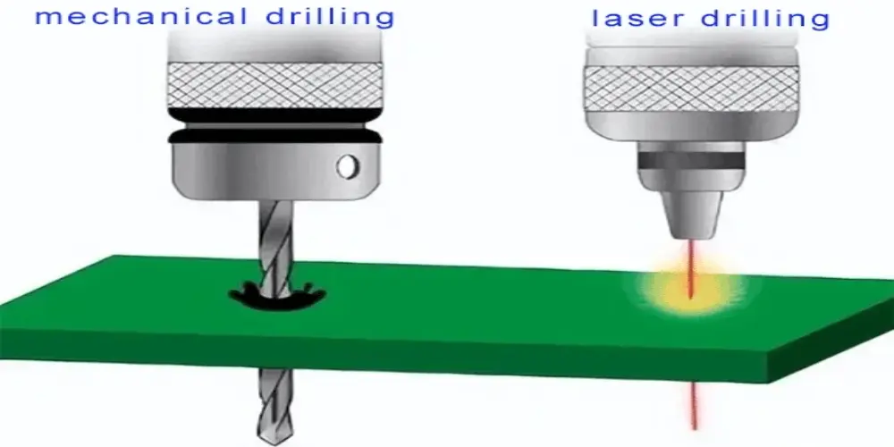
Automatic drilling is controlled by a computer numerical control (CNC) system, which reads the PCB design data through a computer program to perform the drilling process accurately at high speed. The drill head of the PCB drilling machine is designed with an automatic tool-changing system, which accommodates multiple drill bits of varying sizes, enabling precise positioning, quick replacement, and efficient drilling operations. Automatic drilling technology performs well in large-scale PCB production.
Mill Machine Drilling
Milling machine drilling, also called mechanical drilling, is a conventional circuit board drilling technique that is less precise but easier to perform. During the PCB drilling process, the operator manually mounts the drill bit to the milling machine spindle and then guides the drill bit to accurately drill holes in the PCB board. This technique offers excellent flexibility when processing special PCB materials, unconventional hole sizes, and shapes. Milling machine drilling is particularly cost-effective and flexible for small-batch production and prototyping.
Laser Drilling
Laser drilling is a cutting-edge technique that uses a high-powered laser beam to perform non-contact drilling on the PCB, evaporating and ablating the material by the accurate focusing of the laser. The diameter of the laser beam determines the diameter of the hole in the PCB and depth is achieved by control of exposure time. It provides significant advantages of high precision, very small diameter holes, and no degradation of tools and is particularly well adapted to drill microvias in multilayer PCBs.
This drilling method has some disadvantages too, the impossibility of precise control of the hole depth in the absence of a metal stop layer, and burn marks at the hole edge. Laser drilling is more expensive but has turned into an essential technology with its unparalleled accuracy.
Types of Holes Drilled in Circuit Boards
In this section, let’s discuss various kinds of holes, along with their functions. Commonly, it is divided into three categories: via holes, components holes, and mechanical holes.
Via Holes
Vias are tiny holes in PCBs that have been plated with metal. Their main function is carrying electrical signals, power, and ground between different PCB layers.
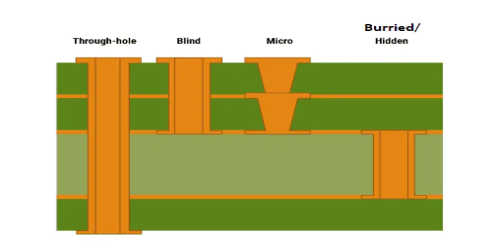
- Through-hole vias run through the entire board from top to bottom, allowing signals to be exchanged between any layers.
- Buried vias are hidden in the inner layers of the PCB, connecting two or more different inner layers. This type of vias takes up less space and is suitable for HDI PCBs, but the manufacturing cost is also high.
- Blind vias are used to interconnect the outer PCB layer with one or more inner layers but don’t go all the way through the board, and they are often used for routing space optimization.
- Microvias are extremely small through holes that are usually drilled using a laser. They are commonly used in HDI PCBs to connect adjacent layers, allowing for more compact designs.
Component Holes
Component holes are used to mount through-hole components, especially high-power components (such as capacitors, resistors, voltage regulators, and op-amps) to provide reliable electrical and mechanical connections and improve heat dissipation.
Mechanical Holes
Mechanical holes are non-conductive holes designed for mechanical assembly on PCBs, mainly used to fix mechanical components such as connectors, brackets, fans, etc. They also help with heat dissipation, guiding heat away from the inner PCB layers. Besides, mechanical holes can help PCBs accurately align with automated manufacturing equipment to streamline production.
How to Drill Holes in PCBs?
This is a complete process that guides you through the precise PCB drilling procedure, where every hole is in the ideal location.
Design Files Preparation
Before PCB manufacturing, the designer typically used PCB design software to finish PCB design. After completing the PCB design, there will be detailed design files. These PCB design files determine the size, location, and other specifications of the holes.
Bare PCB Preparation
The bare printed circuit board is cut to the appropriate size and cleaned to free it from any impurities (dust or oil) before circuit board drilling.
Tool Selection
Select the appropriate drill bit size and type based on the hole specifications. Tool selection is crucial in achieving the proper hole and minimizing material damage.
PCB Fixing
The bare printed circuit board is firmly laid on the drill bed or drill table, and aligned with guides or fixtures to secure it from moving.
Configure Drilling Machine Parameters
During the PCB drilling process, the drilling machine has two key setting parameters (feed rate and rotational speed ) that need to be tailored according to the drill bit size, required hole quality, and PCB material. These settings are optimized to strike the perfect balance between efficient material removal and minimizing risks such as PCB damage, delamination, or tool wear.
Execute the Drilling Operation
Initiate the drill machine, and when the drill head comes in contact with the PCB surface, the drill head starts rotating rapidly while pushing controlled pressure downwards in order to drill through the PCB material and generate the desired hole. In case of multi-layer PCBs, there is an alignment mechanism that allows the drill to pass through several layers simultaneously.
Drilling Cleaning
After PCB drilling, the holes and PCB surface need to be cleared of dust and particles with a soft brush or compressed air.
Hole Inspection
Once PCB drilling is completed, the PCB should be rigorously checked for hole quality using equipment like AOI or X-ray. This is done to ensure the positional accuracy of the holes, the size, and other parameters, thereby ascertaining that there are no costly defects such as additional holes and leaking holes. Given that there is no problem with this verification, the PCB can move to the subsequent step.
Key Factors to Consider When Drilling PCBs
While performing PCB drilling, these are some key factors that need to be kept in mind carefully to achieve optimal circuit board performance.
Right Drill Bit Selection
Choosing the right drill bit type is essential to achieve cleaning and accurate holes.
Common Drill Bits Include:
- Diamond drills: The tip of the diamond drill bit is covered with an industrial-grade diamond coating. With its extremely high hardness and wear resistance, this drill bit is particularly suitable for processing ceramic PCBs or hard materials that are difficult to handle with ordinary drill bits.
- Twist drills: This is the most widely used drill bit for PCB drilling. It has a spiral flute design that can remove material and clear debris while drilling.
- Laser drills: Laser drills are employed to create extremely small holes in high-density PCBs that cannot be drilled using other types of conventional drill bits.
Drill Bit Diameter Determination:
Drill bit diameter is a basic parameter to determine in PCB drilling.
- The drill bit diameter must align with the component lead size. Too small a diameter will make it difficult to insert the lead into the hole, while too large a diameter will result in a loose connection.
- It is essential to maintain an adequate annular ring (the copper pad around the drilled hole) to guarantee reliable soldering.
Aspect Ratio (AR)
Aspect Ratio = Depth of Hole / Diameter of Hole
AR is a hole depth to diameter ratio that defines the copper deposit capability of the hole. It is a key factor that impacts the electroplating process. High AR implies that the through hole has great depth and low diameter, and the plating solution has far to travel to cover the entire inner surface of the hole. It would be hard to cover the hole fully, leading to poor plating. From production experience, the best AR should be:
- Through-hole vias: 10:1
- Microvias: 0.75:1
Drill–to–Copper Clearance
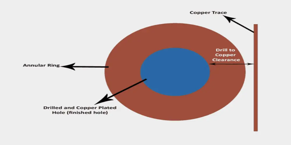
Minimum Drill to Copper Clearance = Annular Ring Width + Solder Mask Web Clearance
The drill-to-copper clearance is the minimum allowable distance between the edge of the drill hole and the nearest copper feature, which can be a trace, pad, or other copper area. This clearance is a critical design parameter to ensure the PCB circuit integrity. Typically given a value of 8 mils or greater, it prevents circuit shorts caused by drill hole position deviations and provides sufficient tolerance for electroplating and solder mask application.
Final Thoughts
Precision PCB drilling results in PCBs with proper connections, structural integrity, and high performance. From selecting appropriate drilling technology to optimizing aspect ratio and drill-to-copper clearance, every decision can have a huge impact on your PCB. As circuit boards continue to miniaturize, the drilling process is more complex and challenging. However, by mastering these PCB drilling basics, coupled with advanced techniques and rigorous inspection, manufacturers can keep PCBs from costly failures.