A good and successful PCB layout design takes more than technical skills, a deep understanding of basic PCB design rules is a must. Even for an experienced engineer or an amateur, learning these 7 PCB design rules will assist you in achieving the optimal PCB layout. In the end, the perfect layout will help you enhance the functionality and dependability of your product. So now we’ll go through each rule in greater detail.
Rule 1: Deciding the Right Board Size and Layer Stackups
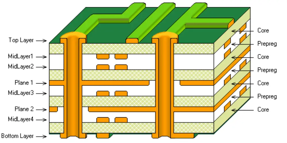
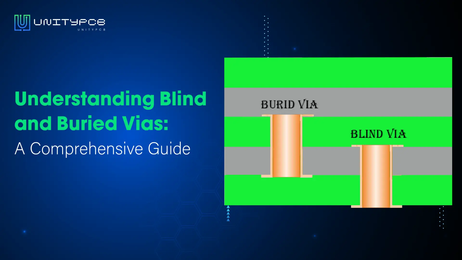
The dimensions of the board and laminate structure need to be established before the beginning of the design. The final size and function of the product place a limitation on the size of the circuit board. If a circuit board doesn’t have enough space to fit all your design requirements, you’ll need to consider the design of a multilayer PCB.

The design of the stack-up is related to the expected functionality of the board and will affect subsequent manufacturing and assembly. Here are a few PCB design rules for stackup to keep in mind.
- Choose the right dielectric material based on frequency, thermal management, and mechanical properties.
- Build a symmetrical stack to minimize warping.
- Use a ground plane for a better result. It will significantly reduce the ground impedance and minimize electromagnetic interference.
- Maintain the minimum distance between the power plane and the ground plane.
Rule 2: Strategically Place Components
In circuit board design, there are many aspects to consider when installing components. Correct placement of components can decrease production costs and speed up the production process. Below we will introduce several useful PCB design rules for component placement.
Grouping components by function
Components with similar functionality should be grouped. Power management components, analog components, and high-speed digital communication components have different signal characteristics and electrical requirements. Component grouping layout can also simplify routing and optimize thermal management.
Prioritize must-have components
First place the components that must be in a specific location, such as connectors and sockets.
Components orientation
Try to place similar components in the same direction for ease of tracing, which will also improve soldering efficiency and reduce assembly errors.
Components spacing
When placing components, do not place them too close together. You need to consider the subsequent assembly process and follow the spacing guidelines between components.
Separating high-power components
Multiple components that generate a lot of heat are placed throughout the board rather than clustered in one location. However, balancing the placement of these components and keeping the traces short is also a challenge.
Centering for easier PCB routing
Placing high-pin-count ICs and large processors in a central location makes routing easier. These components often need to connect to multiple other components, and placing them in the center can shorten tracing lengths and balance the layout.
SMD and THT components design rules
Place all surface mount components on the same side of the board and through-hole components on the top to simplify assembly and subsequent repairs.
Even weight spread across the circuit board
The weight of the entire board is evenly distributed. During the design phase, consider where large components will be placed and make sure they are distributed in different areas. Even weight helps prevent the PCB board from warping or deforming during use.
Rule 3: Place Effective Power and Ground Planes
Circuit boards with more than four layers usually have power layers. Also, even layers are preferred, while odd-numbered layers cannot save costs and may even cause board warping due to asymmetry. In the design of high-speed PCBs, the use of a continuous ground layer can prevent routing traces from passing through ground voids. It’s an important strategy to ensure signal integrity and reduce EMI. The following are some PCB design rules for effective ground and power planes:
- Separate layers are used for the power and ground layers to minimize noise and coupling.
- Place the ground layer adjacent to the signal layer. In high-speed PCBs, the ground layer shields external electromagnetic interference and reduces the impact on high-speed signals.
- Dividing the power plane into multiple areas. It can provide different voltages for various parts on the circuit board to meet the voltage requirements of different components.
- Allow the entire PCB to be covered by the power plane. The fully covered power layer has low a impedance path. It can enable smooth current flow, and avoid local voltage imbalance, and voltage drop.
Rule 4: Essential PCB Design Rules for Trace Routing
In PCB design, routing rules are critical. Following effective PCB design rules for routing can significantly enhance the performance and dependability of circuits.

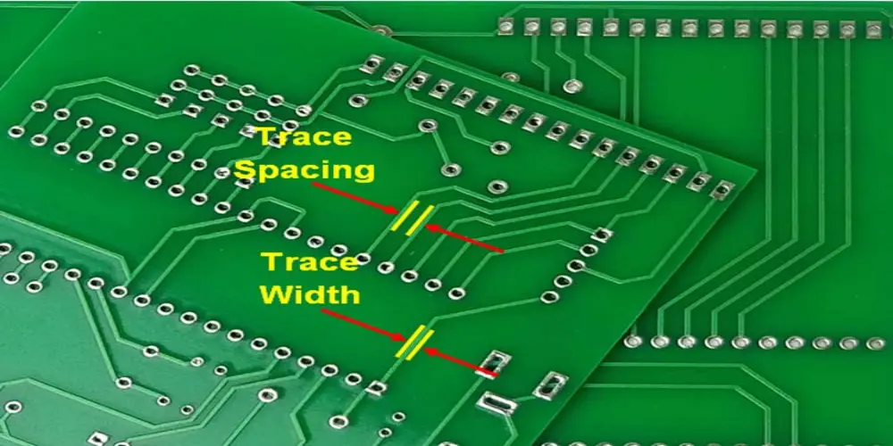
Calculating appropriate trace widths
First, the traces cannot be so thin that they are difficult to produce. Current-carrying capacity is directly impacted by trace width. You need to calculate the appropriate trace width based on the current demand and try to keep the trace uniform during the tracing.
Maintain proper trace spacing to avoid crosstalk
When the routing distance is too close, the coupling of electromagnetic fields may cause crosstalk and affect the integrity of the signal. Before routing, it is best to confirm the correct spacing.
Keep the path the shortest and most direct
Shorter traces can effectively reduce signal loss during transmission. Second, it is easier to maintain impedance consistency and avoid impedance mismatch. Especially on densely routed PCBs, shorter traces can reduce crosstalk between signals.
Avoiding acute and right angles
Acute angle and right angle routing will cause impedance discontinuity, and the signal will be reflected at the bend, affecting the integrity of the signal. When designing, give priority to going straight and avoid turning. If a turn is necessary, consider using two 45-degree turns to form a 135-degree turn to improve signal transmission.
Rule 5: Optimize Thermal Management
Thermal management has an important impact on the reliability and service life of PCBs. Do not place critical components near heat sources. Identify the components that generate more heat and then transfer the heat accordingly. Designers can optimize heat dissipation and prevent overheating of components and the board itself through the layout of heat sinks, thermal vias, thermal pads, etc.
Rule 6: Effective Silkscreen Use for Clear PCB Design

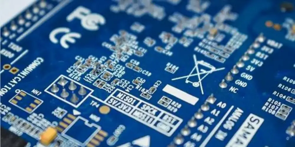
Silkscreen provides key information guidance for subsequent production, assembly, and even maintenance. The following are the PCB design rules for silkscreen to focus on.
Text size
The font size used for silkscreen depends on the type of technique used. The common font needs to be large enough to be easily readable. This ensures that the markings can be clearly read during assembly, inspection, and subsequent repairs.
Placement and alignment
Markings and indicators should be close to components and arranged neatly so that assemblers can identify the model and location of each component at a glance.
Other essential markings
Large BAG components need to have PINs clearly marked. Components such as diodes, capacitors, and transistors need to have the anode and cathode clearly marked. Identification information such as the name of the circuit board, manufacturing date, and version number are usually placed in the corner.
Rule 7: Perform a Design Rule Check (DRC) as Much as Possible
DRC is a tool used during the design process to verify that a design meets specific PCB design rules and standards. It allows designers to identify and resolve problems during the design phase. This tool can check trace spacing, component spacing, minimum trace width, and more.
It takes little time to run the DRC function on the design software. You can check as many times as possible during the design process to minimize subsequent modifications. This saves design and production time to a certain extent and reduces overall costs.
Last Thing
After understanding the 7 PCB design rules, you must have a deeper understanding of how to design an excellent layout. PCB design rules will help you avoid common mistakes that may cause the layout to be compromised. In addition to improving the PCB performance, these design rules simplify the manufacture and subsequent rework. As technology continues to advance, following these PCB design rules will enable you to create more efficient and effective electronic products.


