Quality Control
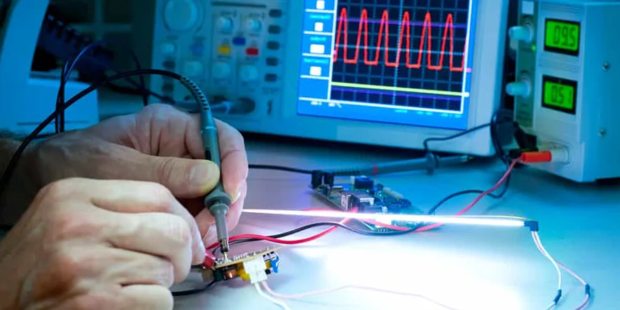
In-circuit testing (ICT) is a widely used PCB testing method to check the quality of electronic components and connections on a PCB. Usually, it is performed at the early stage of the manufacturing process. UnityPCB regards this technology as an important method to verify the functionality and integrity of our products, ensuring the highest quality and reliability of each PCB assembly before delivering to customers.
In-circuit testing is a comprehensive technique for testing PCBs that uses specialized hardware and software tools. It utilizes a “bed of nails” fixture – a multitude of test probes or pins arranged in a grid touching corresponding points of the board. These probes can measure the size of electrical parameters such as resistances, capacitance, inductance, and so on. At the same time, they can detect faults such as short circuits. In the case of ICT, the software part is more tasking as it guides the handling of the hardware as well as the management of test data. One of the major uses of the software is that it schedules the time a node should contact its assigned component, starts the test sequences, and gathers performance and placement information. This is programmable software and the engineers can program according to the requirements of the PCB design. In the testing process, ICT ensures that components have been well mounted and connected, finds problems relating to manufacturing and assembling, and also performs a number of electrical tests. The integration of hardware accuracy and software variability makes ICT a flexible and effective quality control technique in electronics manufacturing, in a position to identify almost any possible failure before its occurrence.

Given proper access to all nodes on the board, ICT can identify around 98% of potential issues. The types of defects that ICT can detect include:
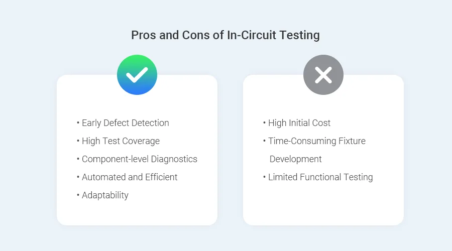
1.Early Defect Detection: In-circuit testing can detect manufacturing faults at a very early stage, requiring minimal rework. As a result, a lot of costs are reduced.
2.High Test Coverage: ICT testing is able to detect 98% of potential issues in a PCB, including short circuits, open circuits, incorrect component values, and wrong component placement.
3.Component-level Diagnostics: In-circuit testing can check each component individually to see if each part functions as intended. Therefore, by using this method, manufacturers can precisely identify the faulty component.
4.Automated and Efficient: ICT is an automated process, which means that a common form of testing large volumes of PCBs can be done at very high speeds.
5.Adaptability: ICT is a widely used testing technique due to its adaptability. The software used in the in-circuit testing process is programmable, so it can be applied to test different PCB designs.
Despite the fact that in-circuit testing has many advantages, we also need to understand the downsides of this PCB testing technique, which include:
1.High Initial Cost: One of the main disadvantages of ICT is that the setup and equipment can be costly especially where the production runs are small. It involves the cost of the fixture, test programming, and the test hardware.
2.Time-Consuming Fixture Development: It is also time-consuming to construct the test fixtures that are required for the ICT, especially when dealing with a complicated board or a densely populated board. This would prolong the time it takes to bring a new product to the market.
3.Limited Functional Testing: As for now, ICT is very effective in identifying component defects, but it is not designed to perform functional testing of the board or system. Other tests may be needed to validate the overall functionality of the board.

ICT is often the first test carried out after the assembly of PCBs but before functional testing and final product integration.
In-circuit testing is most useful on PCBs with through-hole or Surface Mount Technology (SMT) components with test points. However, it may not be effective for specific kinds of boards, including those with a high number of active components per area or with fine pitch parts where accessibility to the test point is limited.
ICT employs a fixed bed-of-nails fixture for testing, which supports high speed as well as parallel testing; however, an individual fixture is needed for every board design. On the other hand, Flying Probe Testing employs probing that is programmable to fly and test the various points of the various designs of the PCBs without the need for the particular fixtures, though more flexible than ICT, they are slower at it.
The time taken for ICT testing can vary with the density of the PCB layer, the number of test points to be probed, and the type of faults that the circuit is being checked on. In total, ICT might take several seconds to a few minutes per single PCB.
Yes, UnityPCB can integrate In-Circuit Testing (ICT) with other testing methods such as Automated Optical Inspection (AOI) and Functional Testing to provide a thorough quality assurance solution for your PCBs.
Elevate Your PCB Quality with UnityPCB's Rigorous Testing Solutions
Contact Us