PCB design greatly impacts the performance, signal integrity, and dependability of the final product. Especially as today’s circuit boards become more complex, compact, and smaller, PCB layout design requires a lot of work and time. Problems like electromagnetic interference, malfunctioning components, board damage, or even total board failure can result from improper circuit board layout. In this article, we will reveal how to design a PCB layout step by step, some useful tips for designing, and common design tools. These will give you some knowledge and background to understand PCB layout.
What Is PCB Layout?
PCB Layout is the process of designing component locations, conductive trace paths, trace widths, and other elements on a printed circuit board to ensure that the circuit board’s signal integrity is maintained and meets the required functionality while optimizing board size. This is the process of translating design concepts into concrete documents that can be used in the production of boards. A successful printed circuit board layout allows for optimal performance.
How to Design PCB Layout: Step-by-Step Explained

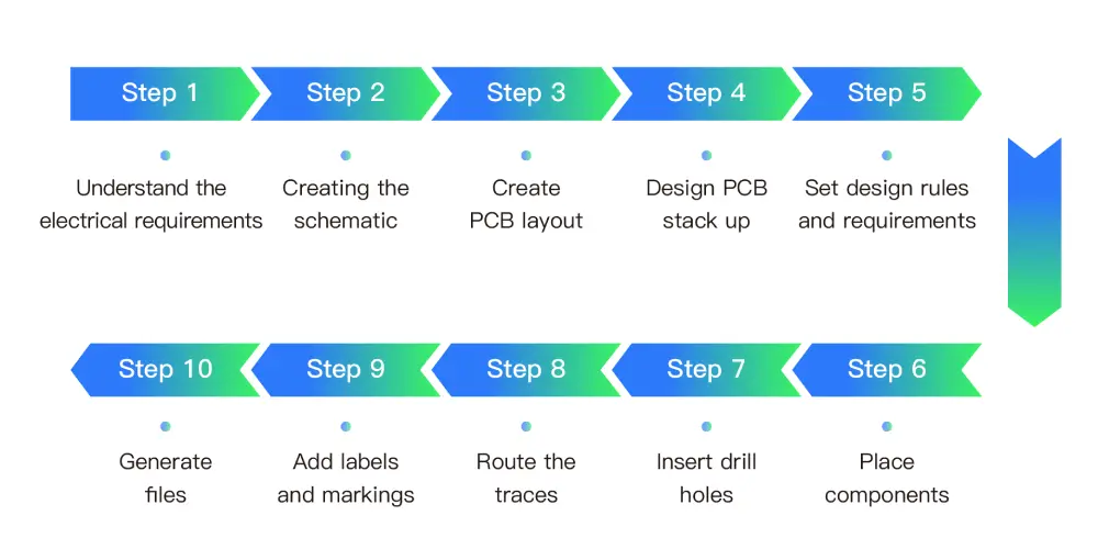
From understanding the electrical specifications of the required PCB to the final documentation, below we will cover the 10 steps in designing a PCB layout.
Step 1: Understand the electrical requirements
Prior to designing, we must comprehend the circuit’s electrical requirements, like the voltage, current requirements, component required, signal frequency, signal type, and so on.
Step 2: Creating the schematic
A schematic is a printed circuit board’s layout blueprint for component placement and alignment. It is a logical way of creating an electronic circuit’s representation. Symbols are used as different components and parameters appear in schematic diagrams and connecting them with lines denotes the connection. This is then used to do circuit simulation to demonstrate that it works electrically as expected.
Step 3: Create PCB layout
Convert schematics into PCB layouts. Select the appropriate PCB size and shape, which takes into account space for mounting, heat dissipation requirements, and fit with other PCBs. Components are shown as footprints with pads and connection lines in the PCB layout. You can see how the components will physically look and be mounted. The software displays air lines that show the electrical connections between components. These lines indicate how the pins of one component should be connected to another component.
Step 4: Design PCB stack up
You can choose the number of layers required depending on how much complex the circuit is. They do slightly different things in every layer. The insulating layer isolates the conducting layer to prevent interference, while the conductive layer transmits power and signals. Accordingly, when the arrangement of the layers has been determined sensibly, the layers’ materials are chosen, depending on how they perform.
Step 5: Set design rules and requirements
There are many PCB design rules, and you can flexibly set the rules to suit the PCB you want to design. It is necessary to ensure the wire spacing and hole spacing, and the appropriate trace width to meet the requirements of current carrying capacity and impedance. There is enough space for soldering components and subsequent repairs. In addition, relevant rules should be set to enable large-scale production based on the manufacturer’s capabilities. These rules need to be adjusted according to actual conditions and are beneficial to the reliability and performance of the PCB.
Step 6: Place components
Each component is placed according to the schematic and layout in order to have each component in the right direction. The heat dissipation of high-power components must be taken into account. Also, the circuit may be divided into different areas depending on the functions. Bringing together components that perform similar functions results in increased signal integrity and decreased interference.
Step 7: Insert drill holes
The drill holes for different types of components require different sizes and locations. For this step, we must think carefully about the component installation requirements. PCB drilling technique and stacking structure will impact the PCB’s dependability and quality.
Step 8: Route the traces
PCB routing needs to minimize interference, improve signal integrity, and meet requirements, like impedance and thermal management. Routing must be optimized in the width of the traces, avoiding sharp corners and right angles, and spacing between traces right.
Step 9: Add labels and markings
Adding labels, markings, and component identification to circuit boards is beneficial to the later PCB assembly and improves production efficiency.
Step 10: Generate files
Before the design is actually delivered, it must also be checked out by way of design rules to make sure that the layout of the circuit board is feasible. When the test is passed, design files can be made to go into production. Gerber files have very detailed information about the PCB and they function as an important bridge, linking the physical design with the final and actual circuit board.
6 Key Tips for a Perfect Circuit Board Layout
Component Placement
Component placement requires many considerations, such as signal integrity, electromagnetic interference, and thermal management. Dividing the circuit into different areas reduces direct interference from different functional modules. Related components can be combined together, and the layout of the circuit board is clearer, as well as convenient for wiring and testing. Combining high-speed components close to and simultaneously near the power supply reduces signal delay and lowers noise.
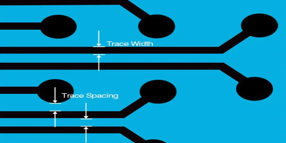
Trace Width and Spacing

Proper spacing is very important to prevent interference, crosstalk, and shorts between adjacent traces. Generally speaking, the greater the current, the wider the trace width. In design software, there are utilities to maintain correct trace width and spacing in PCB layout.
Clearly Silkscreen and Assembly Markings
Providing clear markings and instructions on the silkscreen, including the name, parameters, and other information of each component, is conducive to the correct placement of components by production workers during the assembly process. At the same time, it can also help maintenance personnel to quickly identify and carry out maintenance.
Signal Integrity Consideration
Signal integrity is an important factor in high-speed PCBs. When there is a problem with the signal integrity of the PCB, the PCB will not work as expected. Impedance matching, crosstalk, and reflections in the PCB can cause signal distortion. You can choose some professional design software to detect PCB layout design and ensure signal integrity.
Thermal management
For components that generate a lot of heat, heat dissipation design is required to ensure that they are within a suitable temperature range. Through holes can help components dissipate the generated heat. A heat sink is also a method of transferring heat to a cooling medium.
Design Rules Checking
PCB design rules are the rules that need to be followed for PCB layout, which include electrical design rules, physical design rules, and spacing design rules. The design program checks the design to make sure it satisfies the specifications. Where it does not conform, it can be optimized and adjusted in time to improve the reliability of the design.
4 Popular PCB Board Layout Tools for Engineers and Designers
Altium Designer
This is a very famous software for designing PCBs. It provides a robust component library, an intuitive user interface, and powerful capabilities. Novice users will find this software easy to use, and it is also used by more experienced users. There is a 3D visualization feature that shows the contents of the board in 3D while designing the board is helpful to verify the orientation of the board’s components. It also provides an interesting feature to collaborate teams that makes it easier for design teams to work together and speed up the design process.
Cadence Allegro
A computer-aided design program called Cadence Allegro speeds up the design process by automating wiring, acquiring schematics, and verifying design rules. It has the function of improving manufacturability by optimizing the number of drilled holes, and the positioning of components. The more advanced features of the software are 3D visualization, and the ability to verify design rules. These might enhance the design’s dependability and quality.
KiCad
KiCad is an open-source design software that is free to use. This software is more commonly used by amateurs and small businesses. It can rapidly exchange data with designers using a variety of operating systems, including Windows, Linux, and macOS. KiCad has an active open-source community where users can exchange and access design data.
EasyEDA
It is a free design tool with web page usage. The component library is powerful, allowing users to find the components they need quickly, and then finish their design work. The performance of this software, however, is not suitable for complex PCB designs due to its limited functions.
Concluding Words
PCB layout design is a complex and critical process. Comprehensively, multiple factors such as performance, cost, manufacturability, and so on, should have been considered in the design layout stage. Given the current trend of miniaturization and the great performance of electronic devices today, the PCB layout is designed on smaller boards, which has greater challenges and higher requirements. It is a rigorous and continuously innovative process, which plays a key role in the development of PCB.


