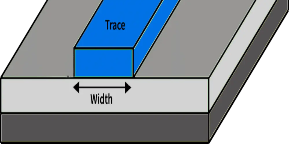
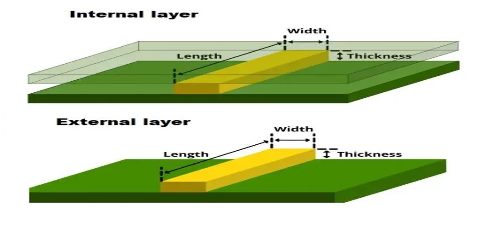
PCB trace width is one of the critical decisions in PCB layout design. It can affect the optimal performance and dependability of electronic devices. Trace width calculation must consider many factors, including current carrying capacity, temperature rise, manufacturing constraints, etc. This guide will bring you through the essential factors that affect the choice of PCB trace width, and discuss how to calculate the ideal width.
What Is PCB Trace Width and Why Is It Important?

A conductive channel etched into the substrate is called a PCB trace. Its function is to link any kind of electrical signal (digital, analog, or power) between two nodes. The connection point of a trace can be a component pin, a trace branch, an empty pad, or a test point. PCB trace width is the width dimension of the conductive path, and it is usually expressed in mils or thousandths of an inch.
PCB trace width directly influences the current that is allowable in the trace. The ideal trace width does not cause heat accumulation. It can effectively help in current flow, thermal management, signal integrity, etc.
What Factors Influence the Choice of Trace Width?
Learn about the importance of trace width, we will deeply explore the 7 key factors to consider when choosing appropriate trace width.

Current Carrying Capacity
The main purpose of tracing is to deal with electrical signals. PCB trace width directly affects the capacity of the trace to conduct current. The trace width should be capable of handling the circuit’s anticipated current without overheating. For those circuits that need higher currents, the widths of the traces should be increased so that the resistance is kept to fairly low levels to ensure that they do not overheat.
Trace Termination
The trace width design usually needs to consider the pad size of its terminal connection. In SOIC packages, the trace width is usually smaller than the pad width. This design can ensure sufficient spacing between adjacent traces and avoid violating the minimum spacing constraint rules.
Impedance Control
In low-frequency circuit boards, the impedance effect is small. In high-frequency circuit boards, impedance is an important factor affecting trace width. High-frequency signals propagate along the traces. The magnetic and electrical fields generated will directly influence the impedance. Signal integrity issues can be addressed by controlling the width of traces.
Thermal Management
The flow of current generates heat. PCB traces can be used as heat dissipation paths for heat generated by components or current flow. These wider traces have more surface area through which they spread heat better. They will not overheat when handling higher currents, reducing the temperature rise on the circuit board.
Copper Weight and Thickness
The thickness as well as the weight of the copper trace also defines the current carrying capacity of the traces. Thicker traces can allow higher currents to pass through, allowing for slim trace width.
Board Space Constraints
PCB size limits space for tracing and also the maximum width that can be traced. For low-power traces, it is recommended to choose a smaller trace width to increase the available routing space. A balance should be made between a trace width sufficient to carry the current and the area available on the board.
Manufacturing Restrictions
The minimum trace width will depend on the manufacturer. The capabilities of the PCB manufacturer must be fully considered to ensure that the selected trace width meets both electrical requirements and can be manufactured. Of course, the fabrication of narrower traces will also be costly and will need better technology and tools.
How to Calculate PCB Trace Width?
The PCB trace width choices can be influenced by numerous things. Next, we’ll look at how to calculate it and pick the best one.
Why Use PCB Trace Width Calculator?
PCB trace width calculator is a professional design tool. It is able to calculate the most suitable PCB trace width based on input design parameters. These parameters include maximum current, ambient temperature, copper thickness, etc. By inputting them into the calculator, designers can obtain recommended trace width values.
PCB trace width calculator can be helpful for designers to find out the best width. Designers can effectively avoid electrical failures, or fire risks by using the calculator. The calculator can simplify complex calculation processes and improve design efficiency. It can help designers consider many variables during the calculating process. This can make the circuit board run normally under various operating conditions.
Calculator Using IPC-2221 or IPC-2152 Standards
There are many trace width calculators based on industry standards. IPC 2221 and IPC 2152 are the two most commonly utilized standards.
IPC-2221 Calculator:
The IPC 2221 calculator uses graphs and formulas to help designers determine the current-carrying capacity of traces in a circuit board. The IPC-2221 standard contains the formula (I=kΔTbAc) for determining the permitted current across a trace.
This formula can then be used to calculate the trace width, which indicates the cross-sectional area that our intended current can safely flow across.
First, calculate the Area:
Cross-sectional Area = (Current / (k × Temperature Rise^b))^(1/c)
Where:
Cross-sectional Area is in square mils (mils²).
Current is in amperes (A).
Temperature Rise is in degrees Celsius (°C).
K value: 0.024 for internal layers, 0.048 for external layers.
1/c is actually 1/0.725, where c=0.725.
Where the constants k, b, and c are determined by fitting the IPC-2221 curve.
Then, calculate the Width:
Trace Width = Cross-sectional Area / (Copper Weight×1.378)
Where:
Trace Width is in mils
Cross-sectional Area is in square mils (mils²)
Copper Weight is in ounces (oz)
1.378 is the conversion factor (mils/oz)
IPC-2152 Calculator:
The IPC-2152 calculator employs a better technical way of calculating the width of the PCB trace. Using this calculator we have to use the computer-integrated generic charts to find the unadjusted cross-sectional area. The calculator takes into account various parameters to calculate the correct trace width. Some of these parameters are thermal conductivity, trace thickness, material, board thickness, and vias, etc.
Common Questions About Trace Width Calculator
QUESTION 1: Can there be a maximum current limit for which a width can be calculated?
ANSWER 1: Yes. The IPC-2221 Calculator has specific ranges of values to use when calculating trace width.
Current Range: 0 to 35 Amps
Trace Width: 0 to 10.16 mm
Copper Thickness: 0.5 oz to 3 oz
Temperature Rise: 10 °C to 100 °C
QUESTION 2: What does temperature rise mean?
ANSWER 2: The difference between the highest safe operating temperature of a PCB and its normal operating temperature is called temperature rise. When the current increases it will create more heat. The rule of thumb for safety says that hiding from the trace temperature rise within 10 °C will guarantee the service life and reliability of most electronic devices.
QUESTION 3: Why do internal traces require wider than external traces?

ANSWER 3: The outer traces feature better heat conduction capabilities since they have heat dissipation via air convection. Dielectric material surrounds the inner traces, with poor heat dissipation characteristics and heat accumulation. Wider inner traces are needed in order to disperse heat and avoid excessive temperature rise. In special environments such as vacuum, and packaged components, the outer layer routing cannot rely on air convection to dissipate heat. All routing at this time should use the width design of the inner layer routing.
Ending Notes
In PCB design, there is careful consideration of PCB trace width. It is essential to the dependability and operation of electronic equipment. The amount of current PCB trace can carry is highly dependent on the trace width. When calculating the trace width, a number of affecting elements must be carefully considered. A good tool for calculating width is the PCB trace width calculator. It can greatly help designers to increase design efficiency. An ideal PCB trace width can be acquired by the calculator considering multiple factors. With a calculation, design accuracy can be achieved as well as PCB reliability.


