A PCB via is a small drilled hole used to electrically connect different PCB layers, enabling signal and power transfer between them. As PCBs become increasingly miniaturized and designs become more complex, choosing the right printed circuit board via is critical. This blog explores five common types of PCB vias and factors to consider when selecting, and helping engineers and designers make informed decisions.
5 Common Types of PCB Vias
Here we present five types of PCB vias that are suitable for different design requirements.
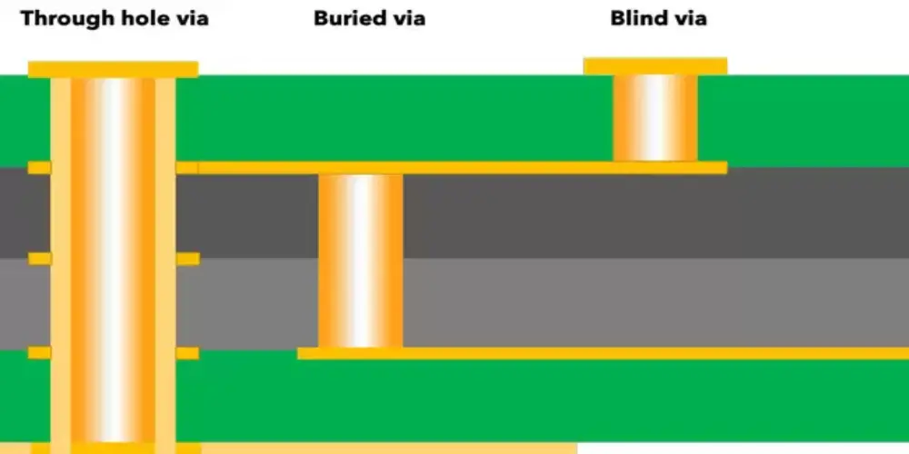
Through-hole Vias
Through-hole vias penetrate from the top to the bottom layer all along the entire PCB. Such circuit board vias are generally used in component mounting holes or inner interconnections. Production is simple as they do not require precise depth control while drilling the PCB.
Through-hole vias possess certain advantages:
Strong Connectivity: Through-hole vias create a strong electrical and mechanical link between PCB layers.
Better Heat Management: Their structure contributes to heat management via the efficient transmission of heat.
Reworking and Testing Access: Due to this PCB via’s access on both sides of the board, the rework and testing would be simpler.
But they have some disadvantages as well:
Larger Drilling Size: The minimum drilling size of through-hole via is typically bigger than other vias, limiting density.
Space Utilization: Through-hole vias take up space on all the layers, reducing the available space for routing.
Signal Integrity Issues: They act as stubs at high frequency, reflecting the signals.
Blind Vias
Blind vias connect from an outer PCB layer (top or bottom layer) to at least one or more inner layers but do not pass completely through the entire circuit board. Compared to through-hole via, this PCB via is only exposed on one side of the circuit board. Blind via hole is challenging to manufacture because of the need to precisely control the depth of the hole. They are usually created using laser drilling or controlled depth drilling, and then electroplating is used to create the electrical connection.
Blind vias provide significant advantages in high-density design:
Efficient Space Utilization: Blind vias do not take up space on all PCB layers, freeing up space for additional PCB traces and components.
Reduced Layer Count and Cost: For complex circuit boards, blind vias can reduce the total number of layers and lower the overall cost of PCB production.
Improved High-Frequency Performance: Shorter PCB via lengths enhance high-frequency performance by reducing parasitic inductance and capacitance.
Flexibility in Design: Layer-to-layer connections can be optimized by PCB designers without affecting the whole stack-up.
Buried Vias
Buried vias connect at least two inner layers in a multilayer PCB and are not visible on the outer layers. They require internal plating prior to applying the two outer layers on the board. This PCB via can be used to form direct connections between specific inner layers, giving designers more design flexibility for complex circuits.
Buried vias have some remarkable advantages:
Enhanced Signal Integrity: Buried vias create more direct and shorter paths between inner layers, which minimizes signal reflections and reduces crosstalk, especially important in high-speed designs.
Improved EMC Compliance: The internal properties of buried vias help suppress electromagnetic emissions, thereby improving overall EMC compliance.
Optimized Space Utilization: Buried vias free up more layout area by reducing the surface and inner layer space occupation, allowing the circuit board to accommodate higher-density components while optimizing routing.
Though there are many advantages, the production of a buried via also has some limitations:
Sequential lamination: The drilling and plating of each set of buried vias must be done separately, and then additional layers need to be laminated. Each additional set of buried vias increases production time and process complexity.
Precise Alignment and Lamination Control: Buried vias must maintain accurate positions at different lamination stages, otherwise signal connection errors may occur. Therefore, high-precision alignment techniques and control of lamination shrinkage and offset are required during manufacturing.
Advanced Inspection Requirements: The buried vias are covered in the inner layer, so high-end inspection equipment such as X-ray inspection is needed to inspect their shape, filling, and connection integrity.
Microvias
Microvias are small vias, typically less than 150 microns in diameter, with the ideal aspect ratio of 0.75:1 (diameter-to-depth ratio) and a depth not more than 0.25 mm. Microvias are commonly used in complex multilayer PCBs to connect adjacent inner layers or surface layers to inner layers. Microvias enable denser and more complex PCB designs, which is very important in HDI designs. These vias on the board play a significant role in PCB miniaturization which is crucial for wearable devices, smartphones, and IoT devices. The following are three common types of microvias:
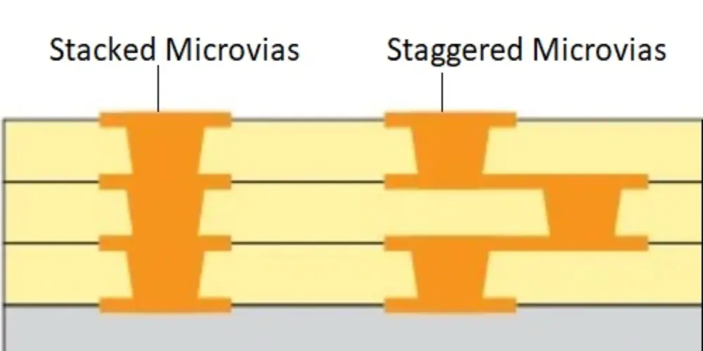
Stacked vias are microvias stacked vertically in layers over one another, creating the interconnection between three or more conductive layers.
Skip vias create links between non-adjacent layers by skipping one or more layers, reducing routing in complex high-density interconnect designs.
Staggered vias involve placing microvias at somewhat offset locations between layers, as compared to being directly stacked vertically like stacked vias.
Via-in-pad
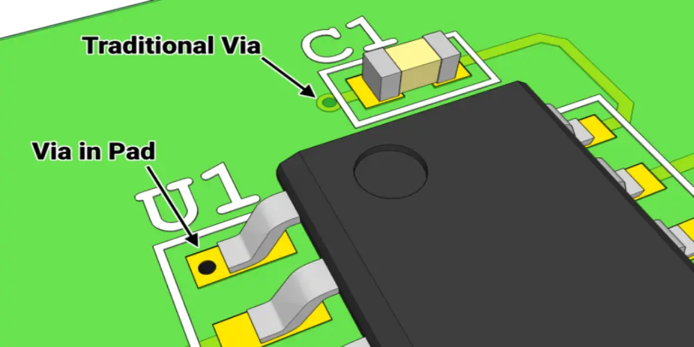
Via in pad is placed directly into the metal pad of a surface mount component, such as fine-pitch BGAs, and is particularly useful in high-density designs. This enables a more direct connection between components and the PCB, reducing trace lengths, improving signal integrity, and enhancing thermal management. The via-in-pad can save space and simplify the routing of critical signals, but it poses soldering difficulties and potential reliability issues.
Key Factors to Consider When Choosing the Appropriate PCB Via
While selecting the right PCB via for the project, it is essential to consider the below 6 factors to deliver the optimal PCB performance, reliability, and manufacturability.
Via Type
Selecting the right via type is critical to achieving optimal inter-layer connectivity. Through-hole vias are suitable for relatively simple designs, while blind and buried vias enhance routing flexibility in multilayer PCBs and microvias are ideal for HDI PCBs. The type of PCB via depends on the complexity of the PCB, signal requirements, manufacturability, and project needs.
Via Size
PCB via size typically varies based on PCB design requirements and manufacturer capabilities. Smaller vias enable higher-density designs but increase manufacturing complexity and cost. While larger vias have greater thermal and electrical conductivity, but occupy more space. A compromise between via size and PCB design requirements (i.e., current-carrying capacity and routing density) is key to achieving a durable and efficient PCB.
Via Tolerance
The circuit board via tolerance determines the acceptable deviation in hole size. PCB manufacturers usually provide internal guidelines that recommend a tolerance range for hole size based on their production process, equipment accuracy, material properties, etc.
Support the Right Technology
Blind and buried vias need to be manufactured using a sequential lamination process, so the design of the PCB stack-up is critical. During the design phase, close communication should be conducted with the PCB manufacturer to rationally design the PCB stack-up and select the appropriate technology to improve the PCB quality and manufacturability.
IPC Guidelines
When designing a PCB via, it is important to follow IPC standards, which include key regulations such as via spacing. Class 2, Class 3, Class 3DS, and military IPC design guidelines are especially crucial, and various IPC levels are appropriate for different application scenarios.
Annular Ring
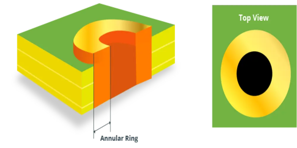
The annular ring is a copper ring around the via, and its size directly affects the reliability and performance of the via. Considering tolerance factors such as material expansion or contraction and drill position deviation, the annular ring needs to maintain sufficient copper area to ensure a stable electrical connection with the trace on a specific layer before the PCB via is plated. IPC Class 2 and Class 3 have different requirements for annular rings, and Class 3 requires stricter tolerance control to ensure stable electrical connections in high-reliability applications.
Typical Uses of Circuit Board Vias
Signal Routing
PCB via is commonly used to direct route signals between different PCB layers. Through-hole via is an adequate solution for most circuit boards. Blind vias and buried vias can be used in more dense designs where there is less space. With properly positioned printed circuit board vias, signals can be effectively transmitted without interference or delay.
Escape Routing
Larger surface mount technology components often use through-hole vias for escape or fan-out routing. Blind vias or microvias are sometimes used, and via-in-pad is used on extremely dense packages like high pin count BGAs.
Power Routing
PCB via for power and ground network is typically restricted to larger through-hole vias as they have the capacity to conduct more current. Blind vias can also be used to save space in high-density designs.
Stitching Vias
These PCB vias establish multiple connections to a plane and are typically implemented as thru-hole or blind vias. For instance, a sensitive circuit area may be enclosed by a metal strip with strategically placed vias linking it to the ground plane for EMI shielding.
Thermal Vias
Thermal vias can effectively diffuse the heat generated by components through the internal copper plane layer, prevent local overheating, and improve the reliability and life of components.
Takeaways
The PCB via directly impacts the circuit board performance, reliability, and manufacturing cost. Designers and engineers should treat PCB via selection as a critical step in the PCB design process since it contributes significantly to the success of the final product. When choosing circuit board vias, the application requirements, the ability of the PCB manufacturer, and industry standards must be taken into consideration to make the optimal choice.