As electronic products continue to miniaturize, the circuit boards at their core are also shrinking. However, small circuit boards are prone to defects during automated assembly, which poses a considerable challenge to production. To improve PCB quality and production efficiency, many manufacturers choose to adopt PCB panelization. So, how does PCB panelization help simplify the production process? This article will assist you find the answer by offering a thorough guide on PCB panelization.
What Is PCB Panelization?
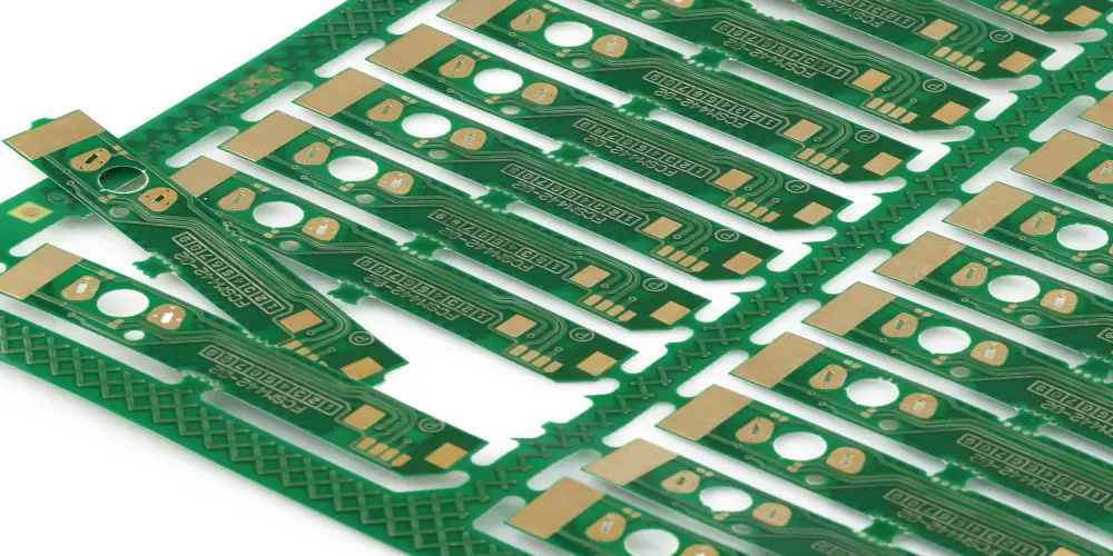
PCB panelization is a technique whereby multiple PCBs are produced on one larger PCB panel for efficient production with less overall cost. This large panel will be easy to move around the assembly line. The PCBs may have the same designs or not in the panel. Once the production is complete, the single PCBs are simply separated from the large PCB panel.
What Are the Types of PCB Panelization?
Here are some PCB panelization types. You can choose different PCB panelization types based on your project requirements.
Order Panelization
Order Panelization is a commonly used PCB panelization method. It refers to the process of combining multiple identical individual PCBs on a PCB panel. Its main advantages are versatility and compatibility, and it can be widely applied to different types of PCBs and manufacturing environments.
Rotation Panelization
This PCB panelization is a method of optimizing material utilization by rotating the PCB. It is mainly used in PCB designs with irregular shapes. The circuit board can be rotated 90 degrees or 180 degrees to achieve optimal space utilization. Due to the different orientations of the PCB, operators constantly need to adjust the working angle. This reduces the assembly efficiency and increases the difficulty of visual inspection quality.
Combination Panelization
This method means combining different types of PCBs into one PCB panel to be produced. It is suitable for products that need many types of PCBs since it can improve their productivity and reduce their cost to deliver quicker. This PCB panelization also possesses a number of challenges. It is difficult to manage product differentiation on the assembly line, which can lead to confusion. If the quality of one board in the combination is not right, then it will have a very strong impact on the production efficiency of the entire PCB panel and reduce overall output.
Popular PCB Depanelization Methods for PCB Panels
It is also very significant to know how to separate an individual circuit board into a PCB panel. Below we will introduce two commonly used PCB depanelization methods.
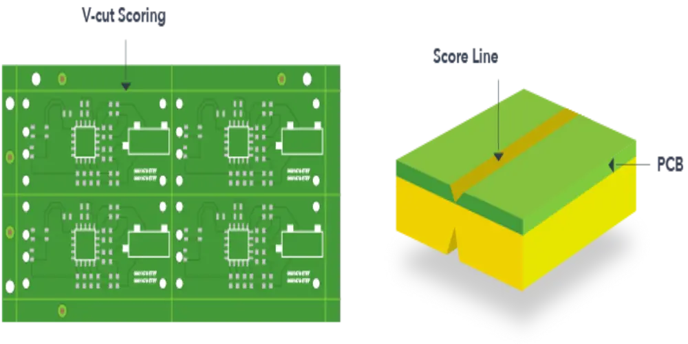
V-Scoring
The process cuts v-shaped grooves on the top and at the bottom of the PCB panel. This normally removes two-thirds of the thickness of the PCB, while one-third thickness of the original is recommended to be the remaining thickness. Depanelization is usually done by a machine since the remaining thickness in the v-groove is enough to provide strength. Manual breaking is not advised, as it may cause excessive stress on the PCB and its components.
It should be noted that the v-score is only can cut straight-line grooves on the panel and hence is not suitable for the processing of PCBs with irregular shapes or complex cuts. Besides, v-scoring is not recommended when some of the components of a PCB are hanging over the edges of the PCB panel.
Tab Routing
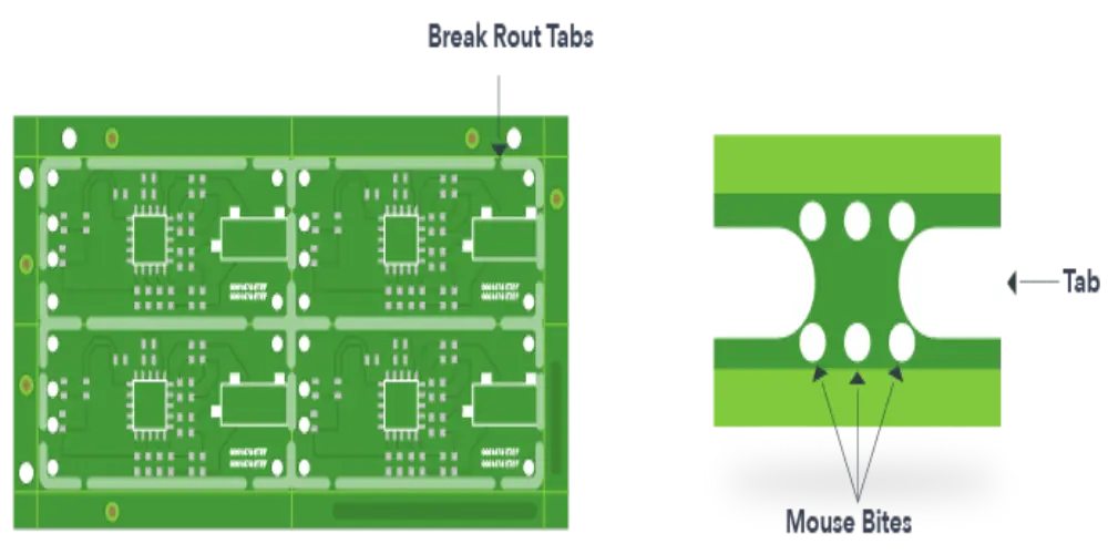
It refers to one method of attaching individual PCBs to the panel frame by giving narrow tabs to the edge of the board. The board would be cut in a routing path with the aid of a specific cutting tool for routing but will leave it with only supporting connecting tabs. It is highly flexible, making it particularly suitable for PCBs with irregular shapes or designs featuring edge-mounted components.
These tabs should be rigid enough to prevent damage to the PCB during assembly and testing but thin enough that later stages can easily separate them from each other. To enhance separation efficiency and minimize damage, perforations or mouse bites are often added to the tabs. These provide uniform distribution of stress, hence enabling smooth detachment either manually or automatically. Tab routing can be more time-consuming and costly compared to other PCB panelization methods. Its versatility makes it a valuable option in PCB manufacturing.
V-Scoring vs. Tab Routing: Which Should You Choose?
Each method has its advantages and limitations, and you need to choose the right one based on your project requirements. Below, we will compare two commonly used methods in a table.
| Aspect | V-Scoring | Tab Routing |
| Board Shapes | Suit for rectangular or square-shaped PCBs | Suit for odd-shaped or complex PCBs |
| Edge Components | Not suitable for edge-hanging components or components near the edges of the board | Allows placing components near the edges of the board, offering more design flexibility |
| Edge Quality | Rough edges, but can be improved with sanding | Small rough edges, can be easily sanded off |
| Material Waste | Wastes less material due to precise cuts | Wastes more material due to more cutting operations |
| Time Use | Requires less time and labor | Requires more time and labor due to complexity |
What Are the Advantages of PCB Panelization?
In this section, we have listed the advantages of PCB panelization. These are the reasons why most manufacturers are prone to choose this technique.
Save Time and Cost
PCB panelization has significant advantages in mass production. This can optimize material utilization, improve equipment utilization efficiency, and reduce labor costs, thereby maximizing production efficiency. Compared to manufacturing each PCB individually, PCB panelization can save production time and significantly reduce overall manufacturing costs.
Enhance Work Efficiency
Multiple individual boards are grouped into a large board and can be processed as a whole in the production process, like assembly, soldering, testing, etc. The more boards you have in your PCB panel, the more efficient your manufacturing will be.
Make Manufacturing Easy
Small circuit boards (smaller than 50*50 mm) are more difficult to manufacture. Grouping them into a PCB panel makes them easier to handle and can reduce manufacturing defects.
Ensure Product Safety
PCB panels can provide effective mechanical protection for individual PCBs. It reduces the risk of damage caused by shock and vibration during assembly.
6 Practical Tips for Successful Circuit Board Panelization
- You need to find the best design that ensures the PCB panel is stable during production and easy to separate There needs to be a balance between easy depanelization and PCB panel strength.
- Be mindful of the positioning of the connectors and components, particularly those that protrude from the board’s edge. This may limit the choice of PCB panelization. For sensitive SMT components near the edge of the board, their orientation and position need to be designed with extra care.
- Rectangular PCBs are usually ideal, but some cases inevitably require complex-shaped PCBs. You can maximize space utilization by rotating the board 90 to 180 degrees to place it in the PCB panel.
- Using the v-score depanelization methods, maintain at least 0.05 inches of clearance between components and the V-groove, with taller components needing to be placed farther away.
- V-grooves can reduce PCB panel integrity. Leading and trailing edge droop can occur as the PCB panel passes through the wave solder machine, causing the panel to warp or get stuck in the wave solder machine. To avoid these problems, designers can reinforce the PCB array by adding jump scoring.
- For the tab routing method, make sure the break tabs are evenly spaced to avoid uneven stress.
UnityPCB Is Here to Meet All Your Needs
PCB panel design affects the quality of a single PCB and is directly related to the overall cost, so a reasonable design is very important. Designers need to comprehensively consider the manufacturability of the PCB panel design, which is usually done with the help of specialized PCB design software. It is also necessary to choose the most appropriate PCB panelization and depanelization method based on the PCB layout and project requirements.
This is where UnityPCB can help you. Our skilled experts can provide you with professional advice. With nearly 20 years of PCB manufacturing experience, UnityPCB provides reliable one-stop PCB & PCBA services. Contact us for a quote, UnityPCB will be your ideal partner!
