In modern electronics, printed circuit boards (PCBs) consist of a number of layers of stacked copper foil circuits. And blind and buried vias are among the most important interconnect solutions when designers have to create connections between these layers. These vias are holes that have been mechanically or lasers drilled, plated with conducting copper to create electrical pathways that allow signals and power to pass between circuit layers.
As we see the growing need of compact and yet sophisticated electronic devices, PCB designers found understanding of blind and buried vias important. This comprehensive guide will guide you through everything you need to know about blind vias and buried vias, their pros and cons, how they differ, and how they are manufactured.
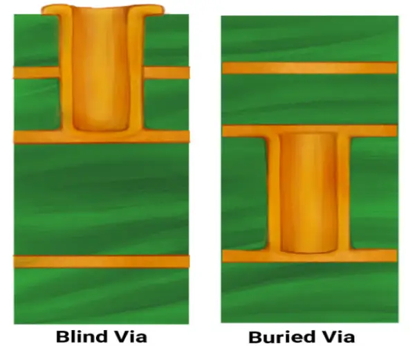
What Is a Blind Via?
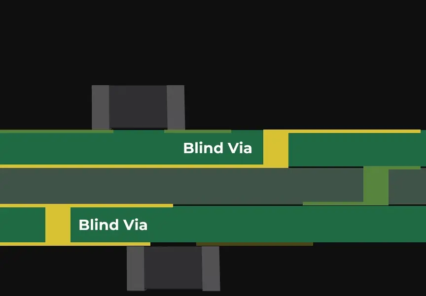
In PCB design, a blind via hole is a specialized electrical connection starting at either the top or bottom surface layer and extending into the board partially, to one or more inner layers without going all the way through to another surface layer. Its name is from its main characteristic, the via is visible only one side of the PCB (blind when looking from the flip side). Designers can make more use of the space available on their circuit boards by using blind vias, which only occupy those layers that need connecting, leaving the others open to provide more routing.
What Is a Buried Via?
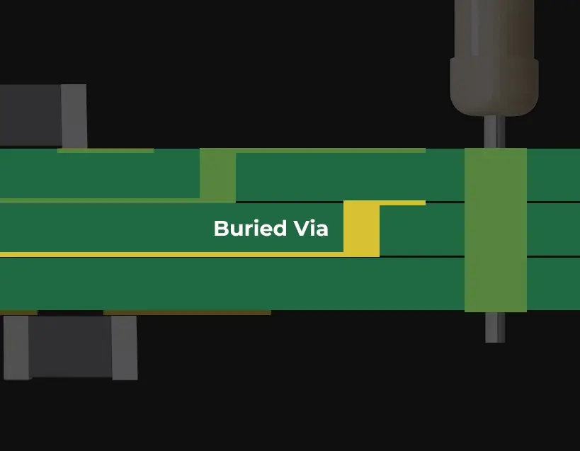
A buried via is a via that connects two or more internal layers of a PCB without reaching the outer layers. As the name suggests, these vias are fully contained within the board and are not visible from the surface. Unlike through holes or blind vias, buried vias cannot be drilled after the PCB has been fully laminated. They need a special manufacturing procedure in which the inner layers are partially bonded, drilled, and finally electroplated before final lamination.
This method is more complex, time-consuming and expensive than blind vias. Nevertheless, it is often used in HDI PCB designs to maximize the available space for other circuit layers.
What’s the Difference between Blind Vias and Buried Vias?
The differences between blind and buried vias are mainly in their placement and connectivity within a PCB. Blind vias connect an outer layer to one or more inner layers without going through the entire board, while buried vias are contained within the inner layers, linking one inner layer to another without extending to the board’s surface.
In essence, blind vias facilitate connections from external components to internal circuitry, optimizing surface space. However, buried vias serve as interconnections between inner layers and allow a clean surface for high density designs.
| Aspect | Blind Vias | Buried Vias |
| Connection | Outer to inner layers | Inner to inner layers |
| Visibility | Visible on one side of the PCB | Not visible on the PCB surface |
| Manufacturing | Requires precision depth-controlled drilling | Requires drilling and lamination between layers |
Benefits and Drawbacks of Blind and Buried Vias
Benefits:
Space Optimization: Using blind and buried vias can save valuable surface space, which allows for compact and efficient layouts.
Improved Signal Integrity: Shorter and more direct signal paths are possible with these vias, reducing signal interference and noise.
Enhanced Design Flexibility: Thanks to these blind and buried vias, designers can make complex interconnections in multilayer PCBs, which is critical in high-density designs.
Drawbacks:
Higher Costs: Blind and buried vias are more expensive than standard through hole vias due to the advanced manufacturing processes involved.
Increased Design Complexity: Blind and buried vias require careful layer planning and precise via placement alongside the management of drill depth and pad control to function properly.
Challenging Rework: These vias are difficult to inspect and repair once implemented, it’s a challenging task to rework after manufacturing.
How Are the Blind and Buried Vias Made?
Blind vias are formed by the controlled- depth drilling process that penetrate an outer layer and reach the target inner layer, with laser drills used for the highest accuracy. The hole depth is critical because a very deep blind via hole can distort or degrade signal, whereas a hole too shallow might not connect completely. Then the holes are electroplated with copper to create conductive pathways.
However, buried vias are fabricated in inner layer fabrication stage before final lamination. The process started by drilling and plating the inner layers individually. Once these pre-processed layers are stacked and laminated together with the additional layers, they make up the entire board. Buried vias are fully enclosed within the PCB and can’t be access or modified once lamination is complete so they must be planned and fabricated early in the process.
Both vias require specialized equipment, multiple lamination cycles and rigorous quality assurance, such as X ray inspection. To prevent extra costs, it is better to consult with your PCB manufacturer when designing a circuit board.
Considerations When Designing Blind and Buried Vias
When incorporating vias into your PCB design, ensure the following guidelines are followed:
- Vias should always extend across an even number of copper layers.
- Vias can’t end on top surface of a core.
- Vias cannot begin on the bottom surface of a core.
- Blind and buried vias must not start or terminate within another via unless one is fully enclosed by the other. This requirement necessitates extra printing cycles, resulting in increased costs.
Conclusion
Indeed, blind and buried vias help a lot when designing compact and high-density boards. However, understanding how to use them properly requires careful planing and advanced manufacturing techniques. Once you have learned their functions and limitations thoroughly, you can unlock the potential of these specialized vias in your PCB designs.
If you’re looking for expert assistance with PCB design or manufacturing, UnityPCB provides industry-leading solutions, including blind and buried via fabrication. Contact us today to discuss your project!