Quality Control
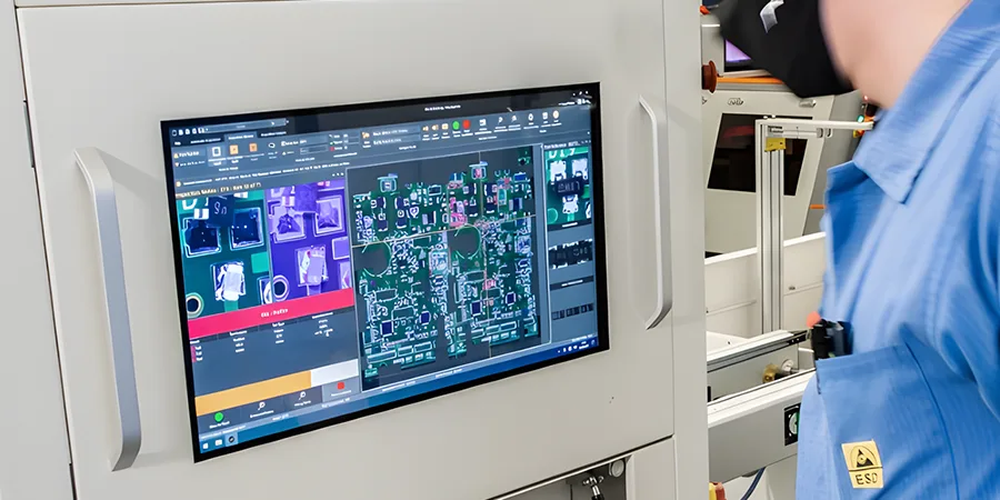
At UnityPCB, Automated Optical Inspection (AOI) is a critical step in our quality control process. We use the state of the art AOI technology, which comes with cutting-edge imaging systems and algorithms to detect faulty circuit boards that a human eye might not detect.
Automated Optical Inspection is a visual inspection method of identifying defects that are likely to happen in the manufacturing and assembly of the PCBs. In this technology, the cameras focused their lenses on the circuit board to inspect the surface features for stains, scratches, opened circuit, and short circuit. Also it can identify lack of components and wrong positions of components .
PCBs will be passed through the AOI machine after all components have been placed on the PCB and again in the final after the soldering process is over. In the process, the several capturing images are produced and used as a golden standard. In further production runs, AOI acquires new image and compares it with the past golden standard image. If it comes across area not in compliance with the standard, it points at probable defects in the area. And then technicians identify these errors and come up with solutions to correct them.
Automated Optical Inspection (AOI) systems rely on 3 key components: lighting, machine vision cameras, and software to processing the acquired data.
1.Lighting is of extreme importance in AOI. LED modules containing red, white, green, and blue lights are utilized in today’s AOI systems for proper and efficient lighting as opposed to incandescent and fluorescent lamps. In addition, its lighting angle addresses issues of different component height to get a proper view of all the parts.
2.High-resolution machine vision cameras are the eyes of AOI systems. With the ability to record as many as millions of pixels in one snap, these cameras can go as high as 100 frames per second. The optical system’s resolution refers to the ability to define the details in an image, and the FOV(field of view) specifies the speed at which AOI scans and the precision of the scanning procedure.
3.The processing software used is actually the commanding control of the AOI system. It also tries to match what is captured against a “golden standard– an idea of what a perfect PCB should be. This standard can be created either by scanning a known good board or by programming according to the specifications of the product. The software can recognize size, shape, position, and quality of each component, checking if there is any issue such as misalignments, solder problems, or missing parts.
All these components work together to accomplish the inspection of printed circuit boards and the identification of defects, ensuring the high quality standards throughout the production process.

Component Flaws
Misaligned Components
Missing Components
Incorrect Components
Tombstoning
Bent or Damaged Leads
Solder Joint Issues
Insufficient solder
Solder Bridges
Excessive solder
Cold Solder Joints
Solder Balling
Lifted Solder Pads
PCB Defects
Short Circuits
Open Circuits
Copper Trace Defects
Scratches and Surface Defects
Etching or plating issues
Marking Flaws
Misaligned Markings
Blurry or Incomplete Markings
Barcode or QR Code Errors
Incorrect or Missing Markings
Automated Optical Inspection delivers a consistent and objective evaluation of the status of printed circuits by using high-resolution cameras and advanced algorithms. While for manual inspection, there is a possibility of human error and the efficiency is relative low.
Yes, AOI can be used on the single and double side PCB as well as multilayer PCBs of different sizes and level of complexity.
Yes, AOI can also be used for BGA inspection but there are limitations such as hard to inspect hidden joints and false negatives and positives.
AOI targets external aspects of PCBs; on the other hand, defects such as solder voids and hidden joints can only be seen through X-ray. X-ray is normally used to check the complicated multilayer board that has internal problem, while AOI is ideal for surface-level inspections.
AOI is usually carried out after the stages of depositing the solder paste on PCB pads, placement of the components and reflow soldering process.
Absolutely, AOI can be used in SMT and through hole assemblies too. It checks for SMT parts for alignment, placement, and solder quality. For PTHs, it checks for soldering and their component orientation.
Elevate Your PCB Quality with UnityPCB's Rigorous Testing Solutions
Contact Us