Single layer PCBs or double layer PCBs are widely used in many devices by simple design and structure. When it comes to complex devices, multilayer circuit boards are usually required, and 4 layer PCB is one of the common choices. These devices demand higher circuit complexity and compactness. In this blog, we will provide a detailed introduction to 4 layer PCB and give you a comprehensive guide.
What Is a 4 Layer PCB?
A 4 layer PCB is a multi-layered circuit board consisting of four conductive layers, alternating with insulating layers. Two outer layers are used for component placement and signal routing, along two inner layers are intended for power distribution and grounding. Due to the increased wiring space and better EMI suppression, 4 layer circuit board is appropriate for high-performance and complicated designs.
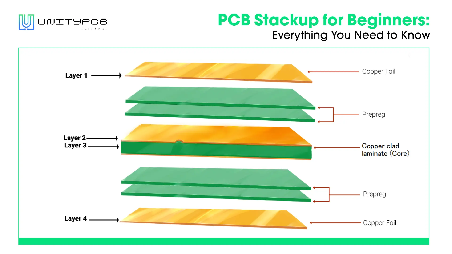
Common 4 Layer PCB Stack-up
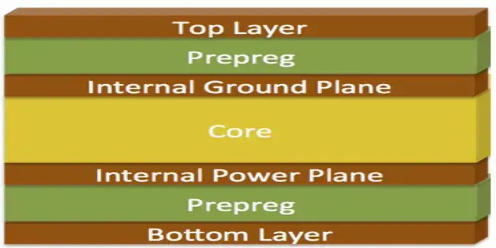
- Top Layer: The first is the signal layer, which is mainly used for component installation and signal routing.
- Inner Layer 1 (Power Layer): The power plane provides stable power to all circuits, reduces power noise, and ensures stable operation of the circuit.
- Inner Layer 2 (Ground Layer): The ground plane provides a return path for the signal, ensuring signal integrity and reducing noise and electromagnetic interference (EMI).
- Bottom Layer: Similar to the top layer, it is also a signal layer used for additional tracing and can be used to mount components, especially in complex circuits.
4 Layer PCB Thickness
The standard thickness of a 4 layer PCB is usually 1.6 mm, but this may vary depending on the specific design and application requirements. 1.2 mm is another commonly used thickness. Factors that affect 4 layer PCB thickness include copper thickness, core material thickness, and prepreg thickness. Copper layers are very thin relative to the total thickness of the PCB, even 3 oz/ft2 copper foil is only 0.105 mm thick. Thus, they are usually not included in the total thickness calculation.
The following formulas more clearly display the thickness of each layer:
- 1.6 mm Total Thickness=0.2 mm(Prepreg)+1.2 mm(Core Material)+0.2 mm(Prepreg)
- 1.2 mm Total Thickness=0.2 mm(Prepreg)+0.8 mm(Core Material)+0.2 mm(Prepreg)
Common Types of 4-Layer PCB Stack-up Designs
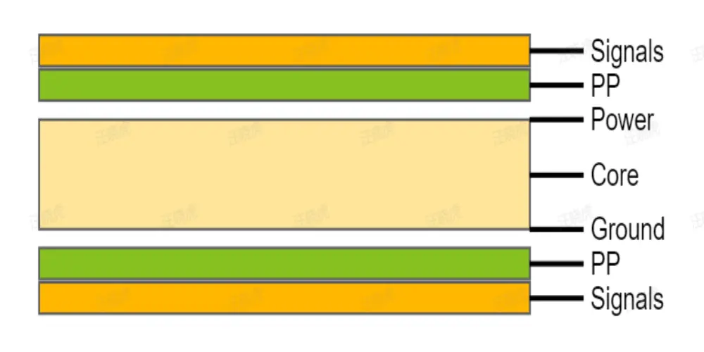
Stack-up 1: Signal-Ground-Power-Signal
The top and bottom signal layers are adjacent to the ground and power planes, providing low-impedance return paths. The power and ground are also close together, thus making a tightly coupled plane pair for stable power distribution and less electromagnetic interference.
Stack-up 2: Signal-Power-Ground-Signal
The power layer is closer to the upper signal layer, which can reduce the voltage drop. Besides that, it provides a more direct current path, whereby high-power devices can acquire a more stable power supply.
Stack-up 3: Ground-Signal-Signal-Ground
The top and bottom layers are ground planes for continuous ground to the signal layer. This will allow for a low-impedance return current path and minimize interference. The middle signal layer and the upper and lower ground layers form a strip wiring structure. This can effectively reduce crosstalk between signals and ensure signal integrity.
Stack-up 4: Signal-Ground-Ground-Power
The two ground layers are arranged adjacent to each other, which has the function of shielding and anti-interference. The power layer provides stable voltage and sufficient current supply to meet the needs of high-power consumption components.
Useful Tips to Design Four Layer Printed Circuit Board
Plan for Proper Layer Stack-up
In a four-layer PCB design, the stack-up structure is crucial, which involves the layout and order of copper and dielectric layers. Above, we also introduced the commonly used stack-up structures. When designing, it is necessary to reasonably layout the power and ground layers, reduce coupling and crosstalk, and optimize the signal path.
Signal Routing Priorities
Prioritize power and ground routing to provide a stable reference plane for subsequent signal routing. For differential pairs, high-speed signals, and key traces, it is important to control impedance, trace width, and spacing to ensure the accuracy of signal transmission. Especially for clock and high-speed signals, their routing should be as short and direct as possible, and impedance matching should be maintained.
Power and Ground Routing
Power plane routing should be of sufficient width to efficiently carry current and minimize voltage drops. By separating and placing power planes adjacent to ground planes, a low-impedance return path is created for signals, significantly reducing electromagnetic interference (EMI) and improving signal quality. High-speed signals should not be routed on the ground or power planes as this can cause signal degradation and noise. Maintaining the continuity of the ground plane is critical to providing a good ground return.
Layered Signal Design
High-speed and sensitive signals should be positioned as close to the reference plane (power or ground layer) as feasible. This lowers the loop inductance of the signal and enhances signal integrity. In order to prevent mutual interference, signals with varying rates and sensitivity levels should be layered.
Ensure Good Thermal Management
Proper placement of thermal vias and optimization of heat dissipation paths is essential. In order to facilitate heat dissipation, thermal vias can be positioned strategically close to heat-generating components, particularly under power components. Heat can be effectively transferred to other layers to promote heat dissipation. Ground vias indirectly support thermal management by helping to transfer heat generated by large components to the ground plane.
Follow DFM Guidelines
Follow the principles of design for manufacturability to ensure that the design complies with the PCB manufacturer’s process and design specifications. This can streamline the manufacturing process, reduce the risk of manufacturing and assembly errors, and improve the reliability and production efficiency of PCBs.
What Are the Advantages of 4 Layer Circuit Boards?
Optimized EMI Shielding
Four layer PCBs can substantially decrease noise, crosstalk, and EMI through specially designed ground layers and power layers. The ground layer serves as a shielding layer, which can reduce electromagnetic wave interference and improve signal stability. The power and ground layer are usually designed to be very close, which achieves a decoupling effect.
Efficient and Reliable Power Distribution
The power layer provides stable and efficient power distribution to the board, helping to reduce voltage drops. The isolated design of the power layer ensures that circuits in different parts of the board receive uniform voltage. It can also minimize the impact of voltage fluctuations and noise.
Higher Component Density and More Compact Design
The 4 layer PCBs have four conductive layers to increase component density, improving efficiency and flexibility in circuit design. It supports more components and complex design than two layer PCBs. The 4 layer PCB also maintains a compact size, making it ideal for electronic products such as laptops, smartphones, and smartwatches.
Cost-Effective Solution
Complexity and cost are balanced in the 4 layer PCB. Compared with PCBs with more layers, they are more cost-effective and easier to design, manufacture, and assemble.
Key Applications of 4 Layer PCB Board
The 4 layer PCB finds wide applications in many industries. It can significantly improve design flexibility and simplify tracing. Below are the major industries and applications of 4 layer PCB.
▪ Consumer Electronics: Computers, Wearable devices, Digital cameras, Camcorders, Smartphones, Laptops, Gaming consoles
▪ Telecommunications: GPS, Satellite, Base station equipment, Routers, Switches
▪ Medical Equipment: X-ray machines, CT scans, Diagnostic equipment, Hearing aids, Patient monitors, Heart Monitors
▪ Automotive: Onboard machines, Headlight switches, Engine sensors, Engine control, infotainment systems, Self-driving enabling equipment
▪ Industrial Controls: Programmable logic controllers, Lighting control, Motor control, Security systems, Automatic conveyor belts, Packaging bots
Choosing UnityPCB as Your Trusted Partner
The 4 layer PCB is one of the most popular circuit board types, offering a balanced combination of performance, design flexibility, and cost. If you are searching for a 4 layer PCB manufacturer, UnityPCB is your trusted partner. With nearly 20 years of experience, UnityPCB is a leading PCB prototype and manufacturing company, specializing in high-quality PCB design, manufacturing, and assembly. We comply with strict quality management standards, ensuring our PCBs meet RoHS, ISO, UL, and IPC certifications. Get a quote from us right now, and we’ll respond promptly.